p.1035
p.1043
p.1051
p.1059
p.1069
p.1076
p.1084
p.1092
p.1099
Anisotropic Effect and the Crystals Nature on the Elastic Fields Dispersal Generated in a Three Layers Material
Abstract:
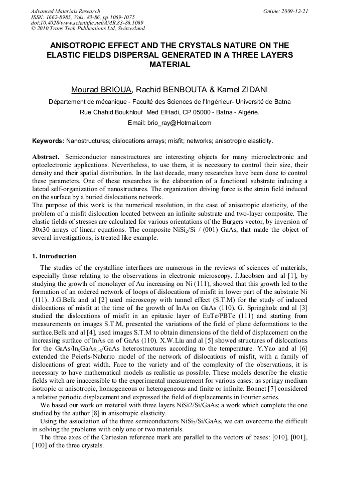
Semiconductor nanostructures are interesting objects for many microelectronic and optoelectronic applications. Nevertheless, to use them, it is necessary to control their size, their density and their spatial distribution. In the last decade, many researches have been done to control these parameters. One of these researches is the elaboration of a functional substrate inducing a lateral self-organization of nanostructures. The organization driving force is the strain field induced on the surface by a buried dislocations network. The purpose of this work is the numerical resolution, in the case of anisotropic elasticity, of the problem of a misfit dislocation located between an infinite substrate and two-layer composite. The elastic fields of stresses are calculated for various orientations of the Burgers vector, by inversion of 30x30 arrays of linear equations. The composite NiSi2/Si / (001) GaAs, that made the object of several investigations, is treated like example.
Info:
Periodical:
Pages:
1069-1075
Citation:
Online since:
December 2009
Authors:
Keywords:
Price:
Сopyright:
© 2010 Trans Tech Publications Ltd. All Rights Reserved
Share:
Citation:


