p.109
p.114
p.119
p.125
p.133
p.139
p.145
p.150
p.155
Analysis and Realization of Critical Points on Hardware Design of FPGA

Abstract:
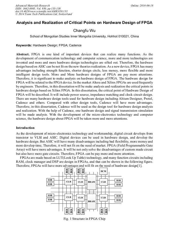
FPGA is one kind of important devices that can realize many functions. As the development of communication technology and computer science, more and more technologies are invented and more and more hardware design technologies are sifted out. Therefore, the hardware design based on ASIC can be not fit on the new theories realization. As a new device, FPGA has many advantages including strength function, shorter design circle, less money, more flexible and more intelligent design tools. More and More hardware designs of FPGA are pay more attentions. Therefore, it is significant to make analysis on hardware design of FPGA. The hardware design for FPGA will be related to the FPGA device. In the market Altera and Xilinx FPGAs are used frequently by engineers. Therefore, in this dissertation will be make analysis and realization the critical points in hardware design based on Xilinx FPGA. In this dissertation, the critical point of Hardware Design of FPGA will be described. It will include power source, impedance matching and clock circuit design. There are many hardware design tools used for hardware design including Altium Designer, Protel, Cadence and others. Compared with other design tools, Cadence will have more advantages. Therefore, in this dissertation, Cadence will be used as the design tool for hardware design analysis and realization. With the help of Cadence, one hardware design and signal transmission simulation will be made analysis. With the development of the micro-electronics technology and computer science, the hardware design about FPGA will be taken more and more attentions.
Info:
Periodical:
Pages:
133-138
DOI:
Citation:
Online since:
June 2014
Authors:
Keywords:
Price:
Сopyright:
© 2014 Trans Tech Publications Ltd. All Rights Reserved
Share:
Citation: