Microstructure and Electrical Properties of Bi3+ Modified ZnO Ceramics

Article Preview

Abstract:

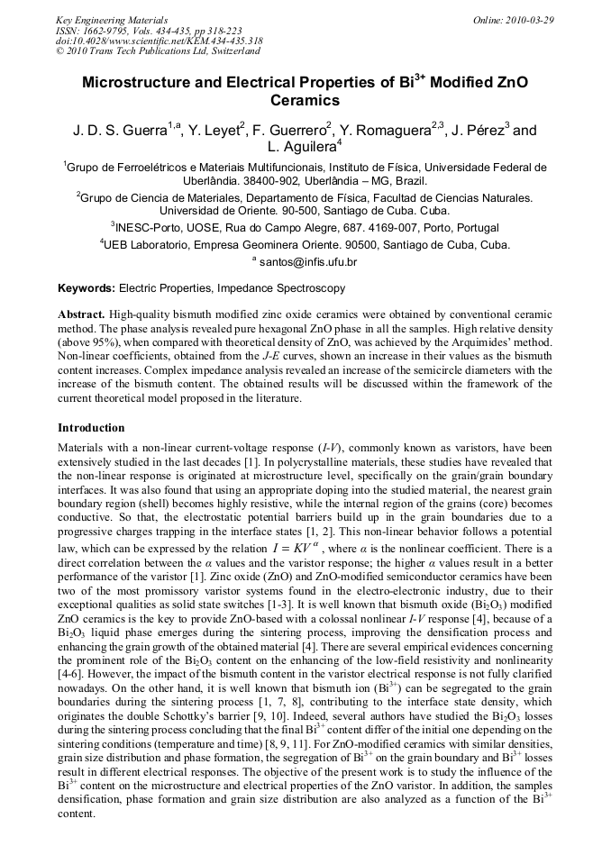
High-quality bismuth modified zinc oxide ceramics were obtained by conventional ceramic method. The phase analysis revealed pure hexagonal ZnO phase in all the samples. High relative density (above 95%), when compared with theoretical density of ZnO, was achieved by the Arquimides’ method. Non-linear coefficients, obtained from the J-E curves, shown an increase in their values as the bismuth content increases. Complex impedance analysis revealed an increase of the semicircle diameters with the increase of the bismuth content. The obtained results will be discussed within the framework of the current theoretical model proposed in the literature.

You might also be interested in these eBooks

Info:

Periodical:

Key Engineering Materials (Volumes 434-435)

Pages:

318-223

Citation:

Online since:

March 2010

Export:

Price:

Permissions CCC:

Permissions PLS:

Сopyright:

© 2010 Trans Tech Publications Ltd. All Rights Reserved

Share:

Citation:

[1] Y.J. Wang, J.F. Wang, H.C. Chen, et al: J. Phys. D: Appl. Phys. Vol. 33 (2000), p.96.

Google Scholar

[2] L.M. Levison and H.R. Philipp: J. Am. Ceram. Soc. Bull. Vol. 65 (1986), p.639.

Google Scholar

[3] R. Einzinger: Annu. Rev. Mater. Sci., Vol. 17 (1987), p.299.

Google Scholar

[4] J. Wong: J. Appl. Phys. Vol. 51 (1980), p.4453.

Google Scholar

[5] T. Takemura, M. Kobayashi, Y. Takada, et al.: J. Am. Ceram. Soc. Vol. 69 (1986), p.430.

Google Scholar

[6] E. Olsson, and G.L. Dunlop: J. Appl. Phys. Vol. 66 (1989), p.4317.

Google Scholar

[7] J.M. Carlsson, B. Hellsing, H.S. Domingos, et al.: Phys. Rev. B. Vol. 65 (2002), p.205.

Google Scholar

[8] J.L. Baptista and P.Q. Mantas: J. Electroceram. Vol. 4 (2000), p.215.

Google Scholar

[9] G. Blatter, and F. Greuter: Phys. Rev. B. Vol. 33 (1986), p.3952.

Google Scholar

[10] N. Yamaoka, M. Masuyama and M. Fukui: Am. Ceram. Soc. Bull. Vol. 62 (1983), p.698.

Google Scholar

[11] M. Bobeth, D. R. Clarke & P. Wolfgang: J. Am. Ceram. Soc. Vol. 82 (1999), p.1537.

Google Scholar

[12] J. Wong: J. Appl. Phys. Vol. 46 (1975), p.1653.

Google Scholar

[13] M. Inada: Jpn. J. Appl. Phys. Vol. 17 (1978), p.1.

Google Scholar

[14] G.E. Pike: Mater. Sci. Technol. Vol. 11 (1994), p.731.

Google Scholar

[15] K.O. Magnusson and S. Wiklund: J. Appl. Phys. Vol. 76 (1994), p.7405.

Google Scholar

[16] M.A. de la Rubia, M. Peiteado, J.F. Fernandez, et al.: J. Eur. Ceram. Soc. Vol. 24 (2004), p.1209.

Google Scholar

[17] M. Žunić, Z. Branković, G. Branković, et al.: Mater. Sci. Forum. Vol. 518 (2006), p.235.

Google Scholar

[18] A.K. Jonscher: Universal Response Law, Chelsea Dielectrics Press. London (1991).

Google Scholar