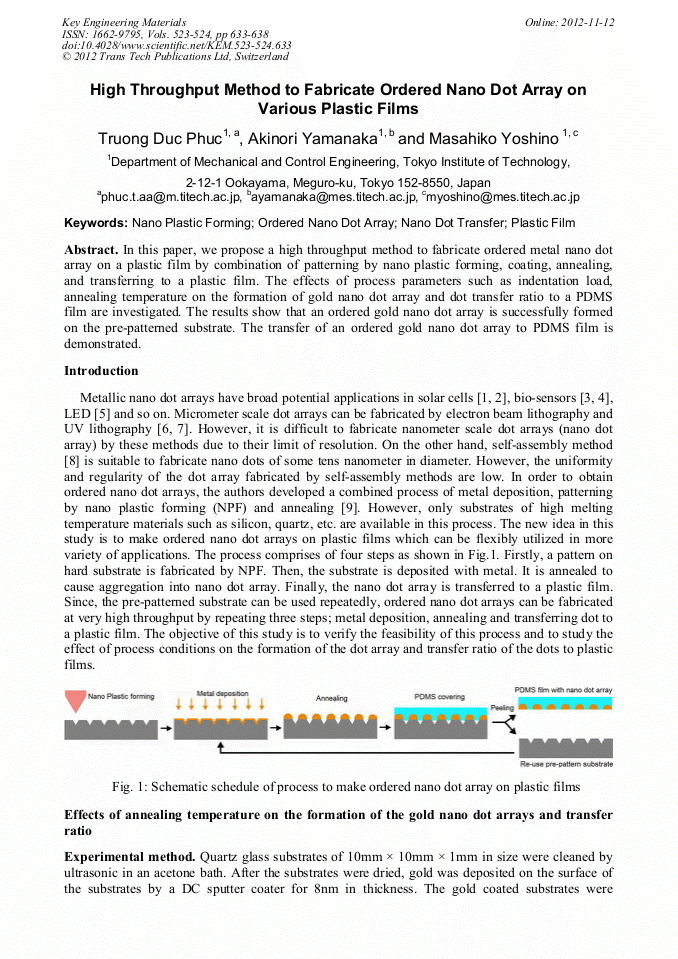
[1]
D. Duche et al, Improving light absorption in organic solar cells by plasmonic contribution, Solar Energy Materials & Solar Cells 93 (2009) 1377–1382.
DOI: 10.1016/j.solmat.2009.02.028
Google Scholar
[2]
K. Nakayama, K. Tanabe, H. A. Atwater, Plasmonic nanoparticle enhanced light absorption in GaAs solar cells, Appl. Phys. Lett. 93 (2008), 121904.
DOI: 10.1063/1.2988288
Google Scholar
[3]
J. Haes, R. P. Van Duyne, A nanoscale optical biosensor: sensitivity and selectivity of an approach based on the localized surface plasmon resonance spectroscopy of triangular silver nanoparticles, J. Am.Chem. Soc. 124 (2002), pp.10596-10604.
DOI: 10.1021/ja020393x
Google Scholar
[4]
A. I. Kuznetsov et al, Laser fabrication of large-scale nanoparticle arrays for sensing applications, Am.Chem. Soc. Nano, 5 (2011), p.4843–4849.
Google Scholar
[5]
P. S. Wong et al, Fabrication and characteristics of broad-area light-emitting diode based on nanopatterned quantum dots, Nanotechnology 20 (2009) 035302.
DOI: 10.1088/0957-4484/20/3/035302
Google Scholar
[6]
S. Y. Chou, P. R. Krauss, P. J. Renstrom, Imprint of sub-25 nm vias and trenches in polymers, Appl. Phys. Lett. 67 (1995), 3114.
DOI: 10.1063/1.114851
Google Scholar
[7]
C.H. Yao, H.Y. Hsiung, C.K. Sung, Influences of process parameters and mold geometry on direct nanoimprint, Microelectronic Engineering 86 (2009) 665–668.
DOI: 10.1016/j.mee.2008.11.056
Google Scholar
[8]
T. Akahane et al, Orientation-controlled and long-range-ordered self-assembled nanodot array for ultrahigh-density bit-patterned media, Japanese Journal of Applied Physics 50 (2011) 06GG04.
DOI: 10.1143/jjap.50.06gg04
Google Scholar
[9]
M. Yoshino, H. Ohsawa, A. Yamanaka, Rapid fabrication of an ordered nano-dot array by the combination of nano-plastic forming and annealing methods, J. Micromech. Microeng. 21 (2011) 125017 (9pp).
DOI: 10.1088/0960-1317/21/12/125017
Google Scholar
[10]
A. V. Grosse, The relationship between the surface tensions and energies of liquid metals and their critical temperatures, J. Inorg. Chem., 1962, Vol. 24, p.147 to 156.
DOI: 10.1016/s0022-1902(62)90147-1
Google Scholar
[11]
D. G. Moore, H. R. Thornton, Effect of oxygen on the bonding of gold to fused silica, Journal of Research of the National Bureau of Standards Vol. 62, No. 3, March 1959.
DOI: 10.6028/jres.062.023
Google Scholar