The Fabrication of Codoped ZnO Thin Films by DC Magnetron Sputtering

Article Preview

Abstract:

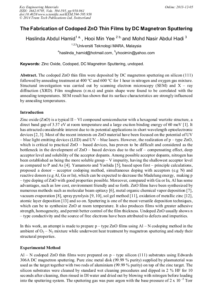
The codoped ZnO thin film were deposited by DC magnetron sputtering on silicon (111) followed by annealing treatment at 400 °C and 600 °C for 1 hour in nitrogen and oxygen gas mixture. Structural investigation was carried out by scanning electron microscopy (SEM) and X ray diffraction (XRD). Film roughness (r.m.s) and grain shape were found to be correlated with the annealing temperatures. SEM result has shown that its surface characteristics are strongly influenced by annealing temperatures.

You might also be interested in these eBooks

Info:

Periodical:

Key Engineering Materials (Volumes 594-595)

Pages:

958-961

Citation:

Online since:

December 2013

Export:

Price:

Permissions CCC:

Permissions PLS:

Сopyright:

© 2014 Trans Tech Publications Ltd. All Rights Reserved

Share:

Citation:

[1] Bagnall D. M, Chen Y, Ko H. J, Park K. T, Hiraga K, Zhu Z. Q, Yao T, Appl. Phys, 84, p.3912, (1998).

Google Scholar

[2] Wong G. K. L, Tang Z. K, Yu P, Kawasaki M, Ohtomo A, Koinuma H, Segawa Y, Appl. Phys. Lett, 72, p.3270, (1998).

DOI: 10.1063/1.121620

Google Scholar

[3] Chen Y. F, Bagnall D. M, Zhu Z, Tao T, Koyama S, Shen M. Y, Goto T, Appl. Phys. Lett, 70, p.2230, (1997).

Google Scholar

[4] S. B. Zhang, S. H. Wei, C. H. Park, Phys. Rev. B, 66, p.73202, (2002).

Google Scholar

[5] T. Yamamoto and H. Katayama Yoshida, Physica B, 302/303, p.155, (2001).

Google Scholar

[6] Bagnall D. M, Chen Y, Zhu Z, Sekiuchi T, Park K, Hiraga K, Yao T, Koyama S, Shen M Y, Goto T, Cryst. Growth , 181, p.165, (1997).

DOI: 10.1016/s0022-0248(97)00286-8

Google Scholar

[7] Smith F. T. J, Appl. Phys, 43, p.1108, (1983).

Google Scholar

[8] El Sayed N, Z, n Kaid M. A, Aly S A, Vacuum, 61, p.1, (2001).

Google Scholar

[9] Banerjee A, Chopra K. L, Major S, Thin Solid Films, 108, p.333, (1983).

Google Scholar

[10] Golgeo N, Cocivera M, Studenikin S. A, Appl. Phys, 83, p.2104, (1998).

Google Scholar

[11] T Ooie, T Nagase, Y Nakatsuka, K Shinozaki, N Mizutani, Jpn. Appl. Phys, Part 2, 39, L713 (2000).

Google Scholar

[12] J Ma, S. L. Cho, Y. K. Kim, Y Sun, G. K. L. Wong, J. B. Ketterson, Appl. Phys. Lett, 75, p.2761, (1999).

Google Scholar

[13] A. Yamada, M. Konagai, Solid State Phenom, 67 - 8, p.237, (1999).

Google Scholar