The Effect of Post-Conventional Thermal Annealing Process on the Photoluminescence Characteristics of Si+-Implanted SiO2 Thin Films

Article Preview

Abstract:

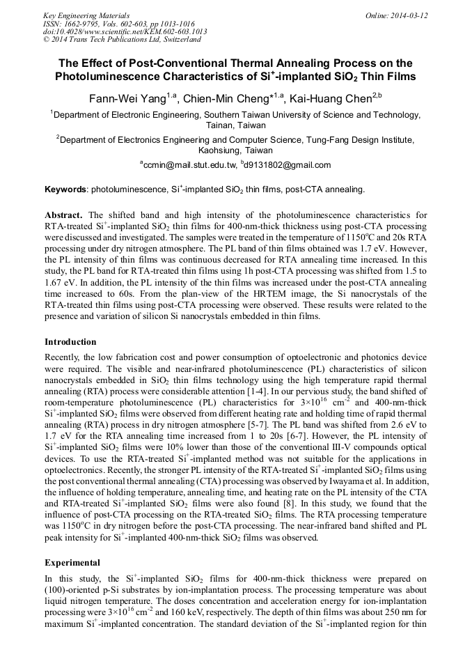
The shifted band and high intensity of the photoluminescence characteristics for RTA-treated Si+-implanted SiO2 thin films for 400-nm-thick thickness using post-CTA processing were discussed and investigated. The samples were treated in the temperature of 1150°C and 20s RTA processing under dry nitrogen atmosphere. The PL band of thin films obtained was 1.7 eV. However, the PL intensity of thin films was continuous decreased for RTA annealing time increased. In this study, the PL band for RTA-treated thin films using 1h post-CTA processing was shifted from 1.5 to 1.67 eV. In addition, the PL intensity of the thin films was increased under the post-CTA annealing time increased to 60s. From the plan-view of the HRTEM image, the Si nanocrystals of the RTA-treated thin films using post-CTA processing were observed. These results were related to the presence and variation of silicon Si nanocrystals embedded in thin films.

You might also be interested in these eBooks

Info:

Periodical:

Key Engineering Materials (Volumes 602-603)

Pages:

1013-1016

Citation:

Online since:

March 2014

Export:

Price:

Permissions CCC:

Permissions PLS:

Сopyright:

© 2014 Trans Tech Publications Ltd. All Rights Reserved

Share:

Citation:

* - Corresponding Author

[1] A. T. Fiory, JOM 57(6), (2005) 21.

Google Scholar

[2] T. S. Iwayama, T. Hama, D. E. Hole, and I. W. Boyd, Vacuum 81, 2 (2006) 179.

Google Scholar

[3] G. A. Kachurin, S. G. Cherkova, D. V. Marin, R. A. Yankov, and M. Deutschmann, Nanotechnology 19, 35, (2008) 355305.

DOI: 10.1088/0957-4484/19/35/355305

Google Scholar

[4] S. T. H. Silalahi, H. Y. Yang, K. Pita, and Y. Mingbinc, Electrochem. Solid-State Lett. 12, 4, (2009) 29.

Google Scholar

[5] M. Y. Fu, J. H. Tsai, C. F. Yang and C. H. Liao, Sci. Technol. Adv. Mater. 9, 4, (2008) 045001.

Google Scholar

[6] J. H. Tsai and M. Y. Fu, Journal of Luminescence. 130, (2010) 1680.

Google Scholar

[7] M. Y. Fu, J. H. Tsai, and C. F. Yang, Optical Engineering. 49, 7, (2010) 073801.

Google Scholar

[8] T. S. Iwayama, T. Hama, D. E. Hole, and I. W. Boyd, Vacuum. 81, (2006) 179.

Google Scholar

[9] M. Nakamura, R. Kanzawa, and K. Sakai, J. Electrochem. Soc. 133, 6, (1986) 1167.

Google Scholar

[10] P. N. Sen and M. F. Thorpe, Phys. Rev. B 15, 8, (1976) 4030.

Google Scholar

[11] N. Sano, M. Sekiya, M. Hara, A. Kohno, and T. Sameshima, "Appl. Phys. Lett. 66, 16, (1995) 2107.

Google Scholar

[12] B. Garrido Fernanedz, M. Lopez, C. Garcia, A. Perez-Rodriguez, and J. R. Morante, J. Appl. Phys. 91, 2, (2002) 798.

Google Scholar

[13] S. T. Chou, J. H. Tsai, and B. C. Sheu, J. Appl. Phys. 83, 10 (1998) 5394.

Google Scholar