Influence of Constant Magnetic Fields on Defect Formation under Conditions of Heat Shock in Surface Layers of Silicon

Article Preview

Abstract:

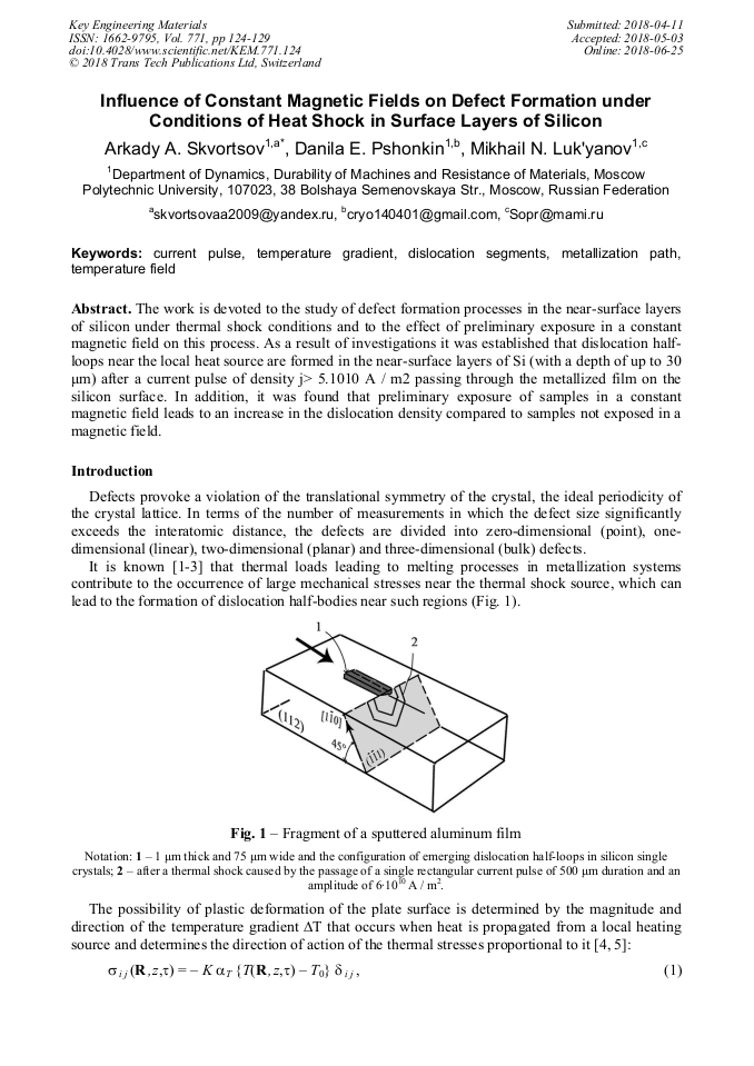
The work is devoted to the study of defect formation processes in the near-surface layers of silicon under thermal shock conditions and to the effect of preliminary exposure in a constant magnetic field on this process. As a result of investigations it was established that dislocation half-loops near the local heat source are formed in the near-surface layers of Si (with a depth of up to 30 μm) after a current pulse of density j> 5.1010 A / m2 passing through the metallized film on the silicon surface. In addition, it was found that preliminary exposure of samples in a constant magnetic field leads to an increase in the dislocation density compared to samples not exposed in a magnetic field.

You might also be interested in these eBooks

Info:

Periodical:

Pages:

124-129

Citation:

Online since:

June 2018

Export:

Price:

Permissions CCC:

Permissions PLS:

Сopyright:

© 2018 Trans Tech Publications Ltd. All Rights Reserved

Share:

Citation:

* - Corresponding Author

[1] C. Ferrari, C. Ghica, E. Rotunno, A study of extended defects in surface damaged crystals, Crystals, Vol. 8, No 2 (2018) 67.

DOI: 10.3390/cryst8020067

Google Scholar

[2] B. Gao, S. Nakano, H. Harada, Y. Miyamura, K., Three-dimensional analysis of dislocation multiplication during thermal process of grown silicon with different orientations, Journal of Crystal Growth 474 (2017) 121-129.

DOI: 10.1016/j.jcrysgro.2016.12.059

Google Scholar

[3] L. Fedina, A. Gutakovskii, A. Aseev, J. Van Landuyt, J. Vanhellemont, Extended Defects Formation in Si Crystals by Clustering of Intrinsic Point Defects Studied by in-situ Electron Irradiation in an HREM, Physica Status Solidi (A) Applied Research. Vol. 171, No 1 (1999).

DOI: 10.1002/(sici)1521-396x(199901)171:1<147::aid-pssa147>3.0.co;2-u

Google Scholar

[4] H. Wang, Q.-H. Qin, The method of fundamental solutions for thermoelastic analysis of functionally graded materials (Book Chapter). Functionally Graded Materials, Nova Science Publishers Inc., New York, (2011).

Google Scholar

[5] А.A. Skvortsov, S.M. Zuev, M.V. Koryachko, V.V. Glinskiy, Thermal shock and degradation of metallization systems on silicon, Microelectronics International. Vol. 33, No 2 (2016) 102-106.

DOI: 10.1108/mi-05-2015-0049

Google Scholar

[6] A.A. Skvortsov, A.M. Orlov, V.E. Muradov, Studying diffusion in multilayer thin-film structures on silicon by the contact melting technique, Technical Physics Letters. Vol. 35, No. 7 (2009) 606-609.

DOI: 10.1134/s1063785009070062

Google Scholar