[1]
J. Kido, M. Kimura and K. Nagai: Science. Vol 267 (1995) p.1332.
Google Scholar
[2]
C.H. Kim and J. Shinar: Appl. Phys. Lett. Vol 80 (2002) p.2201.
Google Scholar
[3]
J. Kido, H. Shionoya and K. Nagai: Appl. Phys. Lett. Vol 67 (2002) p.2201.
Google Scholar
[4]
J. Feng, F. Li, W.B. Gao, S.Y. Liu and Y. Wang: Appl. Phys. Lett. Vol 78 (2001) p.3947.
Google Scholar
[5]
C. Hosokawa, M. Eida, M. Matsuura, K. Fukuoka, H. Nakamura and T. Kusumoto: Synth. Met. Vol 300 400 500 600 700 800.
Google Scholar
[1]
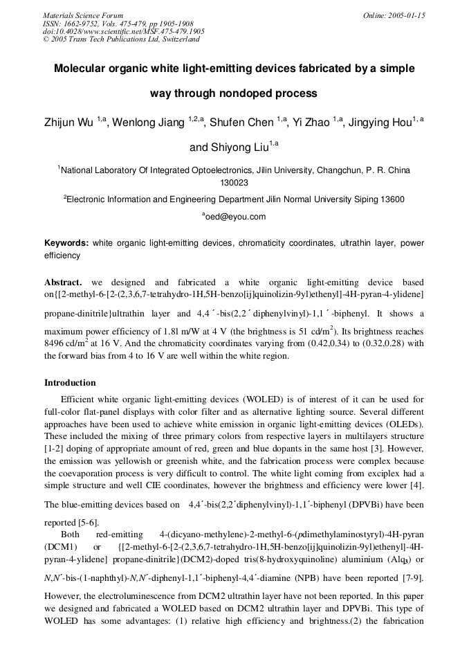
0 device c device a device b DPVBi 456nm DCM2 600nm Normalized intensity (a. u. ) Wavelength(nm) 300 400 500 600 700 800 -0. 01.
Google Scholar
32 0. 34 0. 36 0. 38 0. 40.
Google Scholar
33 increasing bias CIE Y CIE X 7V 10V 13V Intensity (a.U. ) Wavelength (nm) Fig. 2. Normalized EL spectra of the devices having different DPVBi thickness at 13V Fig. 3. EL spectra of device c at 7, 10, 13V, the inset is the CIE coordinates of device (c) from 4 to 16V Fig. 4 Current density-voltage and brightness-voltage characteristics of the device (C), the inset is the power efficiency -voltage characteristics of device (C) 2 4 6 8 10 12 14 16 0 2000 4000 6000 8000 10000 0 200 400 600 800 1000 1200 2 4 6 8 10121416 -0. 5.
DOI: 10.1109/55.82057
Google Scholar
[2]
0 Brightness (cd/m 2 ) Voltage (V) Current density (mA/cm 2 ) power efficiency(lmw -1 ) Voltage (V)91 (1997) p.3.
Google Scholar
[6]
C. Hosokawa, H. Higashi, H. Nakamura and T. Kusumoto: Appl. Phys. Lett. Vol 67 (1995) p.3853.
Google Scholar
[7]
C.W. Tang, S.A. Vanslyke and C.H. Chen: J. Appl. Phys. Vol 65 (1989) p.3610.
Google Scholar
[8]
R.S. Deshpande, Bulvic'V and S.R. Forrest: Appl. Phys. Lett. Vol 75 (1999) p.888.
Google Scholar
[9]
T. Mori, K. Miyachi and Mizutani: J. Phys. D: Appl. Phys. Vol 28 (1995) p.1461.
Google Scholar