p.1880
p.1884
p.1888
p.1892
p.1896
p.1900
p.1904
p.1908
p.1912
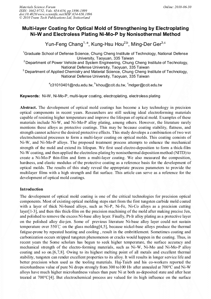
Multi-Layer Coating for Optical Mold of Strengthening by Electroplating Ni-W and Electroless Plating Ni-Mo-P by Nonisothermal Method
Abstract:
The development of optical mold coatings has become a key technology in precision optical components in recent years. Researchers are still seeking ideal electroforming materials capable of resisting higher temperature and improve the lifespan of optical mold. Examples of these materials include Ni-W, and Ni-Mo-P alloy plating, among others. However, the literature rarely mentions these alloys as protective coatings. This may be because coating stability, flatness, and strength cannot achieve the desired protective effects. This study develops a combination of two wet electrochemical processes to form a multi-layer coating on optical molds. This coating consists of Ni-W, and Ni-Mo-P alloys. The proposed treatment process attempts to enhance the mechanical strength of the mold and extend its lifespan. We first used electro-deposition to form a thick-film Ni-W coating, and then applied the electroless plating by nonisothermal deposition method (NITD) to create a Ni-Mo-P thin-film and form a multi-layer coating. We also measured the composition, hardness, and elastic modulus of the protective coating as a reference basis for the development of optical molds. The results of this study reveal the appropriate process parameters to provide the multilayer films with a high strength and flat surface. This article can serve as a reference for the development of optical mold coatings.
Info:
Periodical:
Pages:
1896-1899
Citation:
Online since:
June 2010
Authors:
Keywords:
Price:
Сopyright:
© 2010 Trans Tech Publications Ltd. All Rights Reserved
Share:
Citation:


