p.1193
p.1197
p.1201
p.1205
p.1209
p.1213
p.1217
p.1221
p.1225
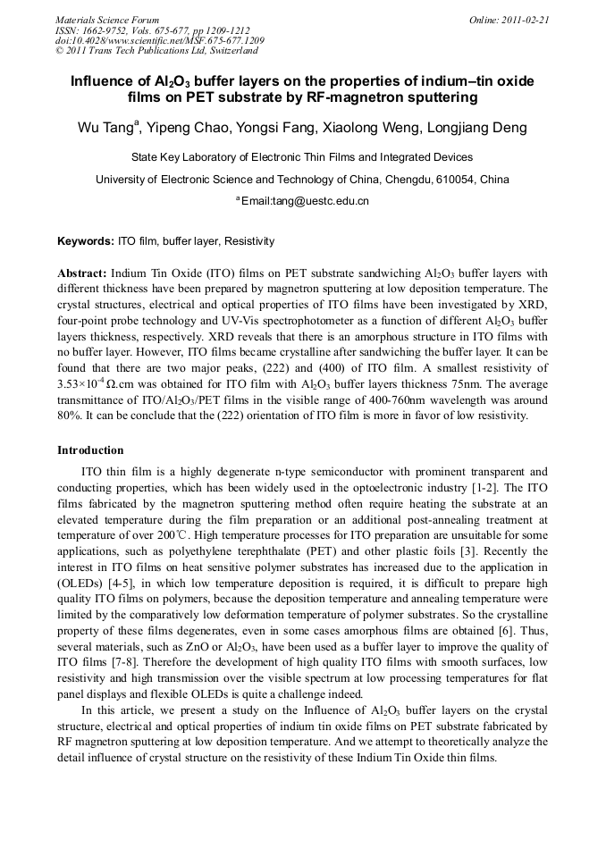
Influence of Al2O3 Buffer Layers on the Properties of Indium–Tin Oxide Films on PET Substrate by RF-Magnetron Sputtering
Abstract:
Indium Tin Oxide (ITO) films on PET substrate sandwiching Al2O3 buffer layers with different thickness have been prepared by magnetron sputtering at low deposition temperature. The crystal structures, electrical and optical properties of ITO films have been investigated by XRD, four-point probe technology and UV-Vis spectrophotometer as a function of different Al2O3 buffer layers thickness, respectively. XRD reveals that there is an amorphous structure in ITO films with no buffer layer. However, ITO films became crystalline after sandwiching the buffer layer. It can be found that there are two major peaks, (222) and (400) of ITO film. A smallest resistivity of 3.53×10⁻⁴ Ω.cm was obtained for ITO film with Al2O3 buffer layers thickness 75nm. The average transmittance of ITO/Al2O3/PET films in the visible range of 400-760nm wavelength was around 80%. It can be conclude that the (222) orientation of ITO film is more in favor of low resistivity.
Info:
Periodical:
Pages:
1209-1212
Citation:
Online since:
February 2011
Authors:
Keywords:
Price:
Сopyright:
© 2011 Trans Tech Publications Ltd. All Rights Reserved
Share:
Citation:


