Physical Chemistry of Water Droplets in Wafer Cleaning with Low Water Use

Article Preview

Abstract:

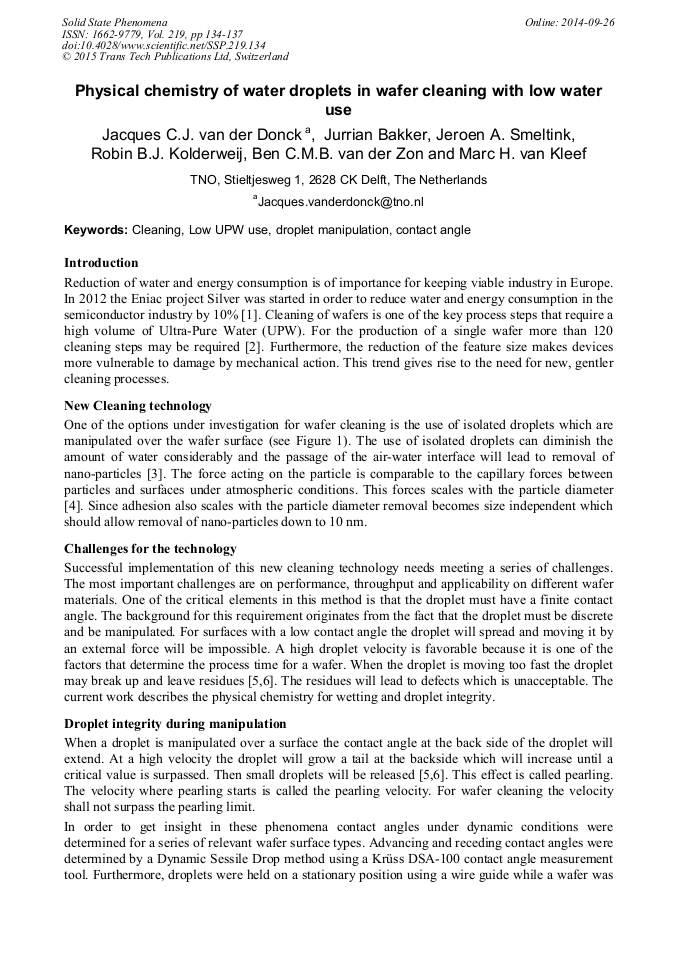
Reduction of water and energy consumption is of importance for keeping viable industry in Europe. In 2012 the Eniac project Silver was started in order to reduce water and energy consumption in the semiconductor industry by 10% [1]. Cleaning of wafers is one of the key process steps that require a high volume of Ultra-Pure Water (UPW). For the production of a single wafer more than 120 cleaning steps may be required [2]. Furthermore, the reduction of the feature size makes devices more vulnerable to damage by mechanical action. This trend gives rise to the need for new, gentler cleaning processes.

You might also be interested in these eBooks

Info:

Periodical:

Solid State Phenomena (Volume 219)

Pages:

134-137

Citation:

Online since:

September 2014

Export:

Price:

Permissions CCC:

Permissions PLS:

Сopyright:

© 2015 Trans Tech Publications Ltd. All Rights Reserved

Share:

Citation:

* - Corresponding Author

[1] Eniac SILVER project (see e. g.: http: /www. silver-project. eu/).

Google Scholar

[2] K.A. Reinhardt, W. Kern, Ed., Handbook of silicon wafer cleaning technology, 2nd ed., William Andrew Inc., New York, (2008).

Google Scholar

[3] A.F.M. Leenaars and S.B.G. O'Brien, Particle removal from silicon substrates using surface tension forces, Philips Journal of Research, Vol. 44, pp.183-209, (1989).

Google Scholar

[4] K.L. Mittal, Coarse on Surface Contamination and Cleaning, Part 2, Hamburg, 27-29, (1998).

Google Scholar

[5] N. le Grand, Nolwenn, A. Daerr, Adrian and L. Limat, Shape and motion of drops sliding down an inclined plane, J. Fluid Mechanics, 541, 293-315, (2005).

DOI: 10.1017/s0022112005006105

Google Scholar

[6] K.G. Winkels, I.R. Peters, F. Evangelista, M. Riepen, A. Daerr, L. Limat and J.H. Snoeijer, Receding contact lines: from sliding drops to immersion lithography, Eur. Phys. J. Special Topics, 192, 195-205 (2011).

DOI: 10.1140/epjst/e2011-01374-6

Google Scholar