Studies on Lead Sulphide (PbS) Thin Film Prepared by Chemical Bath Deposition Method

Article Preview

Abstract:

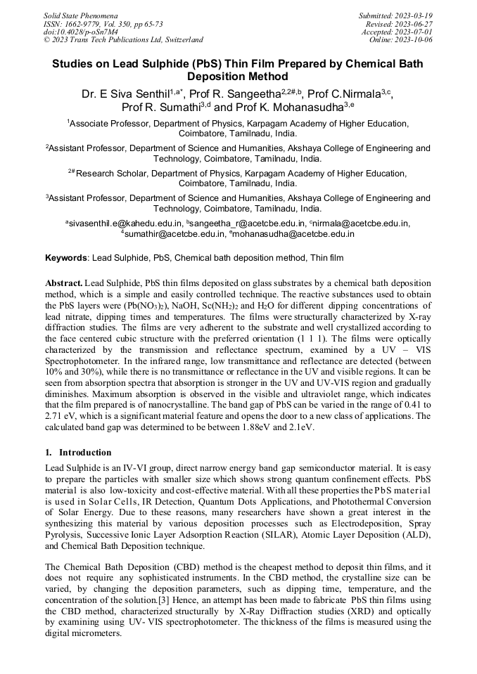
Lead Sulphide, PbS thin films deposited on glass substrates by a chemical bath deposition method, which is a simple and easily controlled technique. The reactive substances used to obtain the PbS layers were (Pb(NO3)2), NaOH, Sc(NH2)2 and H2O for different dipping concentrations of lead nitrate, dipping times and temperatures. The films were structurally characterized by X-ray diffraction studies. The films are very adherent to the substrate and well crystallized according to the face centered cubic structure with the preferred orientation (1 1 1). The films were optically characterized by the transmission and reflectance spectrum, examined by a UV – VIS Spectrophotometer. In the infrared range, low transmittance and reflectance are detected (between 10% and 30%), while there is no transmittance or reflectance in the UV and visible regions. It can be seen from absorption spectra that absorption is stronger in the UV and UV-VIS region and gradually diminishes. Maximum absorption is observed in the visible and ultraviolet range, which indicates that the film prepared is of nanocrystalline. The band gap of PbS can be varied in the range of 0.41 to 2.71 eV, which is a significant material feature and opens the door to a new class of applications. The calculated band gap was determined to be between 1.88eV and 2.1eV.

You might also be interested in these eBooks

Info:

Periodical:

Solid State Phenomena (Volume 350)

Pages:

65-73

Citation:

Online since:

October 2023

Export:

Price:

Permissions CCC:

Permissions PLS:

Сopyright:

© 2023 Trans Tech Publications Ltd. All Rights Reserved

Share:

Citation:

* - Corresponding Author

[1] J.J Valenzuela-Jaregui, R.Ramirez-Bon, A.Menodoza-Galvan, M.Sotelo-Lerma, Optical Properties of PbS thin films chemically deposited at different temperature, Thin film solids, 441 (2003) 104-110.

DOI: 10.1016/s0040-6090(03)00908-8

Google Scholar

[2] Ileana Pop, Cristina Nascu, Violeta Ionescu, E.Indrea, I.Bratu, Structural and optical properties of PbS thin films obtained by chemical deposition, Thin solid films 307(1997) 240-244.

DOI: 10.1016/s0040-6090(97)00304-0

Google Scholar

[3] S. Seghaier, N Kamoun, R.Brini and A R Amara, Structural and optical Properties of PbS thin films deposited by chemical bath deposition, Materials Chemistry and Physics, 97(2006) 71-80.

DOI: 10.1016/j.matchemphys.2005.07.061

Google Scholar

[4] E. Pentia, L.Pitilie, I. Matei, T. Botila and E. Ozbay, Journal of Optoelectronics and Advanced Materials Vol 3, No 2, June 201, 525-530.

Google Scholar

[5] A.Popa, M.Lisca, V. Stancu, M.Buda, E.Pentia, T. Botila, Crystallite size effect in PbS thin films grown on glass substrate by chemical bath deposition, Journal of Optoelectronics and Advanced Materials Vol 8, No 1, Feb 2006, 43-45.

Google Scholar

[6] P.K Basu, T.K Chaudhiri, K.C Nandi, R.S Saraswat, Preparation and Characterization of Chemically Deposited Lead Sulphide thin films, Journal of Material Science 25(1990) 4014 - 4017.

DOI: 10.1007/bf00582474

Google Scholar

[7] Goswami A 2005, Thin film fundamentals, New Age International Publishers, New Delhi.

Google Scholar

[8] Culllity.B D and Stock S R, 2001, Elements of X-Ray Diffraction, Prentice Hall, New Jercey 07458.

Google Scholar

[9] Basu.P.K, Chaudhuri.T.K, Nandhi.K.C, Saraswat R.S. and Acharya.H.N,1990, Preparation and Characterization of Chemically deposited Lead Sulphide thin films, Journal of Material Science and Subject: Chemistry and Material Science and Engineering, Vol 25, No.9 PP-4014-4017.

DOI: 10.1007/bf00582474

Google Scholar

[10] P.K. Nair et al, 1989, Prospects of chemically deposited metal chalcogenide thin films for solar control application, J.Phys, D: Appli.Physics Vol22, PP 829-836.

DOI: 10.1088/0022-3727/22/6/021

Google Scholar