Fault Current Detection Based on Neural Network in Hybrid Circuit Breaker
p.887
p.887
Analysis of Influence Factors on Strength of Mudstone with Soft-Hard Alternant Strata in Nanning Basin
p.891
p.891
Study on the Controlling System of Particle Materials Separating Device
p.895
p.895
An Empirical Study on Value Functions of Stock Markets
p.899
p.899
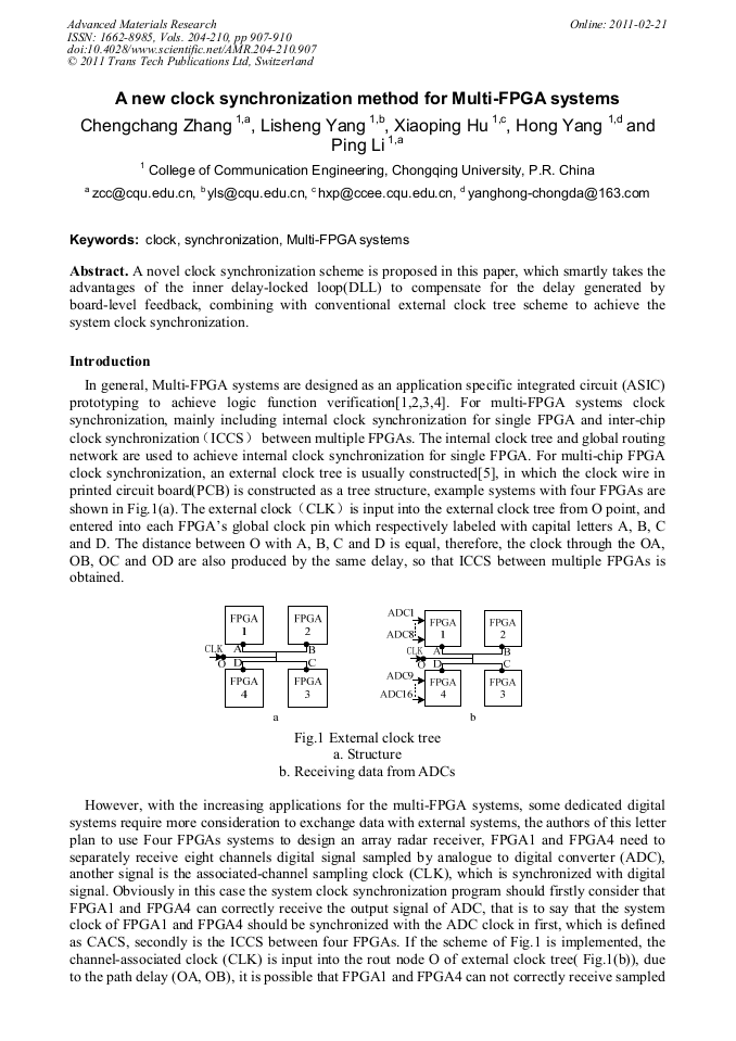
A New Clock Synchronization Method for Multi-FPGA Systems
p.907
p.907
Study on the Decision-Making of Coal Industry Technology Development Based on AHP
p.911
p.911
Ordering Policy for Deteriorating Items with Short Shelf Life Based on Lateral Transshipment
p.915
p.915
Study of the Properties of Poly-P-Phenylene-Benzimidazole-Terephthalamide Fiber Material
p.919
p.919
Theoretical Research for Short Pile
p.924
p.924
A New Clock Synchronization Method for Multi-FPGA Systems

Abstract:
A novel clock synchronization scheme is proposed in this paper, which smartly takes the advantages of the inner delay-locked loop(DLL) to compensate for the delay generated by board-level feedback, combining with conventional external clock tree scheme to achieve the system clock synchronization.
You might also be interested in these eBooks
Info:
Periodical:
Advanced Materials Research (Volumes 204-210)
Pages:
907-910
Citation:
Online since:
February 2011
Authors:
Keywords:
Price:
Сopyright:
© 2011 Trans Tech Publications Ltd. All Rights Reserved
Share:
Citation: