p.2957
p.2961
p.2966
p.2970
p.2974
p.2978
p.2982
p.2987
p.2991
MOSFET Performance Manufactured on <100> Silicon Wafer Using CESL Strain Technology with Temperature Effect

Abstract:
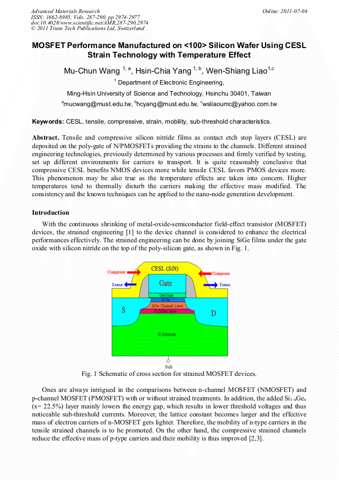
Tensile and compressive silicon nitride films as contact etch stop layers (CESL) are deposited on the poly-gate of N/PMOSFETs providing the strains to the channels. Different strained engineering technologies, previously determined by various processes and firmly verified by testing, set up different environments for carriers to transport. It is quite reasonably conclusive that compressive CESL benefits NMOS devices more while tensile CESL favors PMOS devices more. This phenomenon may be also true as the temperature effects are taken into concern. Higher temperatures tend to thermally disturb the carriers making the effective mass modified. The consistency and the known techniques can be applied to the nano-node generation development.
Info:
Periodical:
Pages:
2974-2977
Citation:
Online since:
July 2011
Authors:
Keywords:
Price:
Сopyright:
© 2011 Trans Tech Publications Ltd. All Rights Reserved
Share:
Citation: