Influence of Annealing Temperature on Nanocrystalline ZnO Thin Films Prepared by Sol-Gel Dip Coating Method

Article Preview

Abstract:

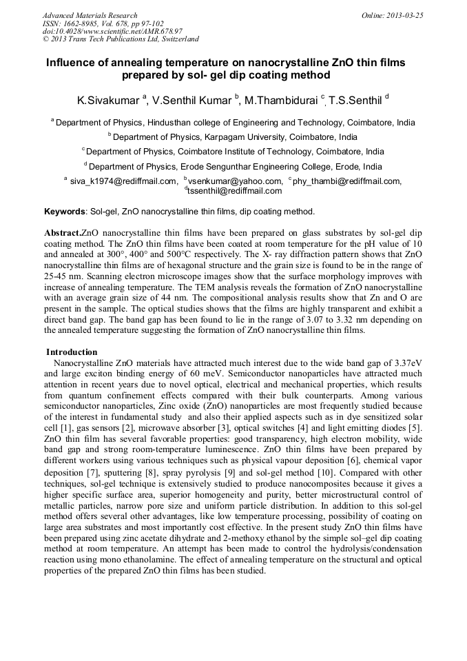
ZnO nanocrystalline thin films have been prepared on glass substrates by sol-gel dip coating method. The ZnO thin films have been coated at room temperature for the pH value of 10 and annealed at 300°, 400° and 500°C respectively. The X- ray diffraction pattern shows that ZnO nanocrystalline thin films are of hexagonal structure and the grain size is found to be in the range of 25-45 nm. Scanning electron microscope images show that the surface morphology improves with increase of annealing temperature. The TEM analysis reveals the formation of ZnO nanocrystalline with an average grain size of 44 nm. The compositional analysis results show that Zn and O are present in the sample. The optical studies shows that the films are highly transparent and exhibit a direct band gap. The band gap has been found to lie in the range of 3.07 to 3.32 nm depending on the annealed temperature suggesting the formation of ZnO nanocrystalline thin films.

You might also be interested in these eBooks

Info:

Periodical:

Pages:

97-102

Citation:

Online since:

March 2013

Export:

Price:

Permissions CCC:

Permissions PLS:

Сopyright:

© 2013 Trans Tech Publications Ltd. All Rights Reserved

Share:

Citation:

[1] Jih-Jen Wu, Guan-Ren Chen, Hung-Hsien Yang, Chen-Hao Ku, Jr-Yuan La, Appl. Phys. Lett. 90 (2007) 213109.

Google Scholar

[2] Jin Chen, Jin Li, Jiahui Li, Guoqing Xiao, Xiaofeng Yang , J. Alloys. Compd. 509 (2011) 740.

Google Scholar

[3] Z.W. Zhou, W.M. Peng, S.Y. Ke, H. Deng, J. Mater. Proc. Technol. 89-90 (1999) 415.

Google Scholar

[4] H. Kind, H.Q. Yan, B. Messer, M. Law, P.D. Yang, Adv. Mater. 14 (2002)158.

Google Scholar

[5] K. Kim, J.S. Horwitz, W.H. Kim, A.J. Makinen, Z.H. Kafafi, D.B. Chrisey, Thin Solid Films 420-421 (2002) 539.

DOI: 10.1016/s0040-6090(02)00836-2

Google Scholar

[6] J. Kouam, T. Ait-Ahcene, A.G. Plaiasu, M. Abrudeanu, A. Motoc, E. Beche, C. Monty, Solar Energy 82 (2008) 226.

DOI: 10.1016/j.solener.2007.07.008

Google Scholar

[7] X.H. Wang, R.B. Li, D.H. Fan, Applied Surface Science 257 (2011) 2960.

Google Scholar

[8] Zhonghai Zhang, Md. Faruk. Hossain, Takuya Arakawa, Takakazu Takahashi, Journal of Hazardous Materials 176 (2010) 973.

Google Scholar

[9] R. Ayouchi, D. Leinen, F. Martín, M. Gabas, E. Dalchiele, J. R. Ramos-Barrado Thin Solid Films 426 (2003) 68.

Google Scholar

[10] Fahrettin Yakuphanoglu, J. Alloys Compd. 507 (2010) 184.

Google Scholar

[11] M. Maleki, M. Sasani Ghamsari, Sh. Mirdamadi and R. Ghasemzadeh, Semiconductor physics, Quantum Electronics & optoelectronic 10 (2007) 30.

Google Scholar