Memory Devices Based on the Nanoparticle Silicon Floating Gate Double-Barrier Structure

Article Preview

Abstract:

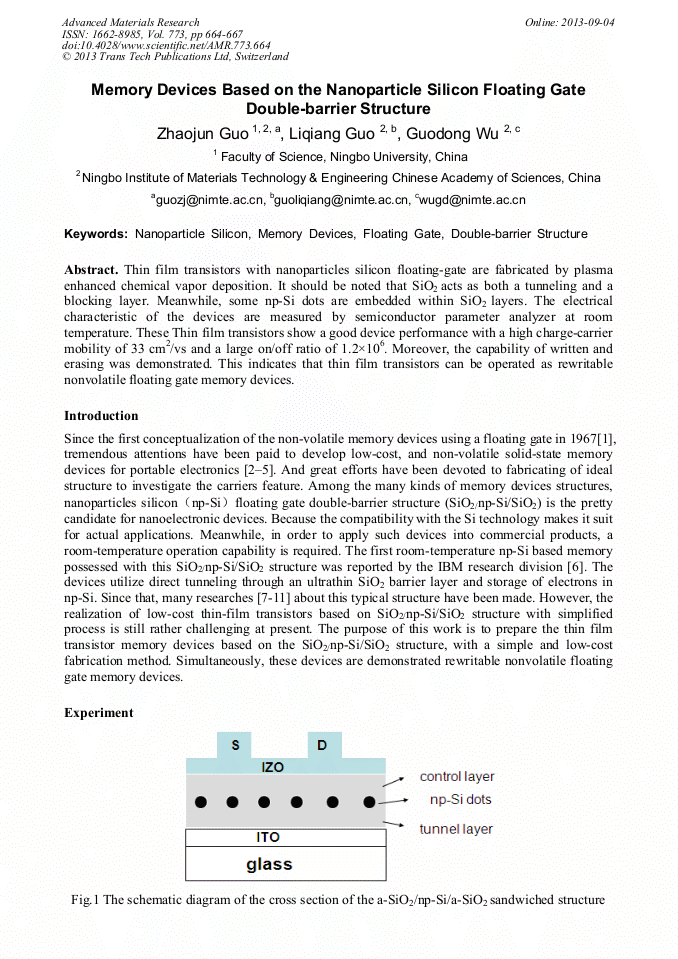
Thin film transistors with nanoparticles silicon floating-gate are fabricated by plasma enhanced chemical vapor deposition. It should be noted that SiO2 acts as both a tunneling and a blocking layer. Meanwhile, some np-Si dots are embedded within SiO2 layers. The electrical characteristic of the devices are measured by semiconductor parameter analyzer at room temperature. These Thin film transistors show a good device performance with a high charge-carrier mobility of 33 cm2/vs and a large on/off ratio of 1.2×10⁶. Moreover, the capability of written and erasing was demonstrated. This indicates that thin film transistors can be operated as rewritable nonvolatile floating gate memory devices.

You might also be interested in these eBooks

Info:

Periodical:

Pages:

664-667

Citation:

Online since:

September 2013

Export:

Price:

Permissions CCC:

Permissions PLS:

Сopyright:

© 2013 Trans Tech Publications Ltd. All Rights Reserved

Share:

Citation:

[1] D. Kahng, S. M. Sze, Bell System Technical Journal Vol. 46 (1967), 1288 b) D. Kahng, IEEE Trans. Electron Dev. Vol. 23 (1976), 655.

Google Scholar

[2] T. Rueckes , K. Kim , E. Joselevich , G. Y. Tseng , C. L. Cheung ,C. M. Lieber , Science Vol. 289 (2000), 94.

Google Scholar

[3] R. Waser, Nanoelectronics and Information Technology, Wiley-VCH Weinheim, (2005).

Google Scholar

[4] J. Sarkar, S. Tang, D. Shahrjerdi, S. K. Banerjee, Appl. Phys. Lett. Vol. 90 (2007), 103 512.

Google Scholar

[5] M. H. R. Lankhorst, B. Ketelaars, R. A. M. Wolters, Nat. Mater. Vol. 4 (2005), 347.

Google Scholar

[6] S. Tiwari, F. Rana, H. Hanafi, A. Hartstein, E. F. Crabbe, and K. Chan, Appl. Phys. Lett. Vol. 68 (1996), 1377.

Google Scholar

[7] S. Banerjee, S. Y. Huang, T. Yamanaka, and S. Oda, J. Vac. Sci. Technol. B Vol. 20 (2002), 1135.

Google Scholar

[8] S. Y. Huang, S. Banerjee, R. T. Tung, and S. Oda, J. Appl. Phys. Vol. 93 (2003), 576.

Google Scholar

[9] A. Nakajima, T. Futatsugi, K. Kosemura, T. Fukano, and N. Yokoyama, J. Vac. Sci. Technol. B Vol. 17 (1999), 2163.

Google Scholar

[10] Y. Shi, K. Saito, H. Ishikuro, and T. Hiramoto, J. Appl. Phys. Vol. 84 (1998), 2358.

Google Scholar

[11] D. N. Kouvatsos, V. Ioannou-Sougleridis, and A. G. Nassiopoulou, Appl. Phys. Lett. Vol. 82 (2003), 397.

Google Scholar

[12] J. S. Lee , Y. M. Kim , J. H. Kwon , H. Shin , B. H. Sohn , J. Lee , Adv. Mater. Vol. 21 (2009), 178.

Google Scholar