Properties Study of ZnS Thin Films Fabricated at Different Substrate Temperatures by Pulsed Laser Deposition

Article Preview

Abstract:

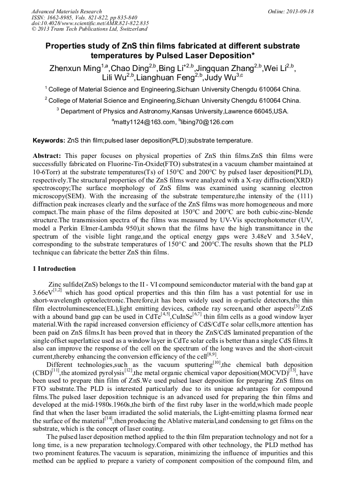
This paper focuses on physical properties of ZnS thin films.ZnS thin films were successfully fabricated on Fluorine-Tin-Oxide(FTO) substrates(in a vacuum chamber maintained at 10-6Torr) at the substrate temperatures(Ts) of 150°Cand 200°Cby pulsed laser deposition(PLD),respectively.The structural properties of the ZnS films were analyzed with a X-ray diffraction(XRD) spectroscopy;The surface morphology of ZnS films was examined using scanning electron microscopy(SEM). With the increasing of the substrate temperature,the intensity of the (111) diffraction peak increases clearly and the surface of the ZnS films was more homogeneous and more compact.The main phase of the films deposited at 150°C and 200°C are both cubic-zinc-blende structure.The transmission spectra of the films was measured by UV-Vis spectrophotometer(UV,model a Perkin Elmer-Lambda 950),it shown that the films have the high transmittance in the spectrum of the visible light range,and the optical energy gaps were 3.48eV and 3.54eV,corresponding to the substrate temperatures of 150°C and 200°C.The results shown that the PLD technique can fabricate the better ZnS thin films.

You might also be interested in these eBooks

Info:

Periodical:

Advanced Materials Research (Volumes 821-822)

Pages:

835-840

Citation:

Online since:

September 2013

Export:

Price:

Permissions CCC:

Permissions PLS:

Сopyright:

© 2013 Trans Tech Publications Ltd. All Rights Reserved

Share:

Citation:

* - Corresponding Author

[1] Yano S, Schroeder R, Ullrch B, Sakai H. Absorption and photocurrent properties of thin ZnS films formed by pulsed-laser deposition on quartz. Thin Solid Films 2003; 423: 276-273.

DOI: 10.1016/s0040-6090(02)01037-4

Google Scholar

[2] Yong SK, Sun JY. Studies on polycrystalline ZnS thin films grown by atomic layer deposition for electroluminescent application. Applied Surface Science 2004; 229: 111-105.

DOI: 10.1016/j.apsusc.2004.01.050

Google Scholar

[3] Kashani H. Production and evaluation of ZnS thin film by the MOVCD technique as alphaparticle detectors [J]. Thin Solid Films,1996, 288(1):50.

DOI: 10.1016/s0040-6090(96)08845-1

Google Scholar

[4] Isaiah O,Oladeji,Lee C. Synthesis and processing of CdS/ZnS multilayer films for solar cell application [J]. Thin Solid Films,2005, 474(1-2):77.

DOI: 10.1016/j.tsf.2004.08.114

Google Scholar

[5] Idris A,Salih K,Ferhunde A. Some physical properties of chemically sprayed Zn1-xCdxS semiconductor films [J]. Material Science in Semiconductor processing,2007, 10(2-3):103.

DOI: 10.1016/j.mssp.2007.04.001

Google Scholar

[6] Asenjo B,Chaparro A M,Gutierrez M T. Study of CuInS2/buffer/ZnO solar cells,with chemically deposited ZnS-In2S3 buffer layers [J]. Thin Solid Films,2007, 515(15):6036.

DOI: 10.1016/j.tsf.2006.12.056

Google Scholar

[7] Akira I,Masahi H,Takuya A. Ultrasonic chemical bath deposition of ZnS(O,OH) buffer layers and its application to CIGS thin -film solar cells[J].Solar Energy Materials and Solar cells, 2006, 09, (18-19):3130.

DOI: 10.1016/j.solmat.2006.06.032

Google Scholar

[8] Green M.Third generation photovoltaics:solar cells for 2020 and beyond [J].Physica E, 2002,14,65.

Google Scholar

[9] Anderson N G.Proposal for a new superlattice-based solar cell structure [J].Solar Energy, 1993,50(2):27.

Google Scholar

[10] Varitioms T E,Tust ison R M.Ion beam sput tering of ZnS thin films [J].Thin Solid Films, 1987,151(1):27.

Google Scholar

[11] Gangopadhyay U,Kyunghae K,Mangalaraj D.Low cost CBD ZnS antireflection coating on large area commercial mono-crystalline silicon solar cells [J].Applied Surface Science, 2004, 230(1-4):364.

DOI: 10.1016/j.apsusc.2004.02.059

Google Scholar

[12] Afifi H H,Mahoud S A,&Ashour A.Structural study of ZnS thin films prepared by sprary pyrolysis[J].Thin Solid Films,1995, 263(2):248.

DOI: 10.1016/0040-6090(95)06565-2

Google Scholar

[13] Dona J M,Herreo J.Chemicial bath codeposited CdS/ZnS films characterization[J].Thin Solid Films,1995,268(1):5.

DOI: 10.1016/0040-6090(95)06738-8

Google Scholar

[14] Perez D,Lewis L J.Phys.Rev.Lett,2002, 89(25):255504.1.

Google Scholar

[15] L.I. Berger Semicond. Mater., 1997 (1997).

Google Scholar

[16] J.I. Pankove, Optical Processes in Semiconductor, Dover, New York, 1971, p.34.

Google Scholar