Surface Morphology and Optical Property of Silver Nanoparticle Thin Film Prepared by Electrostatic Spray Deposition

Article Preview

Abstract:

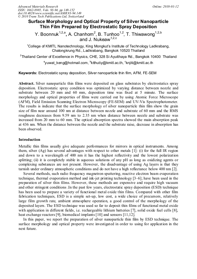
Silver nanoparticle thin films were deposited on glass substrates by electrostatics spray deposition. Electrostatic spray condition was optimized by varying distance between nozzle and substrate between 20 mm and 60 mm, deposition time was fixed at 5 minute. The surface morphology and optical properties of films were carried out by using Atomic Force Microscope (AFM), Field Emission Scanning Electron Microscopy (FE-SEM) and UV-Vis Spectrophotometer. The results is indicate that the surface morphology of silver nanoparticle thin film show the grain size of film near around 100 nm at distance between nozzle and substrate of 60 mm and the RMS roughness decreases from 9.59 nm to 2.35 nm when distance between nozzle and substrate was increased from 20 mm to 60 mm. The optical absorption spectra showed the main absorption peak at 436 nm. When the distance between the nozzle and the substrate raise, decrease in absorption has been observed.

You might also be interested in these eBooks

Info:

Periodical:

Advanced Materials Research (Volumes 93-94)

Pages:

149-152

Citation:

Online since:

January 2010

Export:

Price:

Permissions CCC:

Permissions PLS:

Сopyright:

© 2010 Trans Tech Publications Ltd. All Rights Reserved

Share:

Citation:

[1] M.L. Scott, P.N. Arendt, R.W. Springer, R.C. Cordi, W.J. McCreary, in: H.E. Bennett, A.H. Guenther, D. Milam, B.E. Newman (Eds. ): Damage in Laser Materials, Nat. Bur. Stand. (US) Spec. Publ., Boulder, Colorado, Vol. 746 (1987), p.419.

Google Scholar

[2] N. Thomas, A. Erlandson, J. Farmer, H. Gregg, C. Marshall, W. Siekhaus, J. Wolfe, D. Fix, D. Ahre, in: H.E. Bennett, A.H. Guenther, M.R. Kozlowski, B.E. Newnam, M.J. Soileau (Eds. ): Laser-Induced Damage in Optical Materials, Proceeding of SPIE, Boulder, Colorado, Vol. 3578, (1999).

DOI: 10.1117/12.344462

Google Scholar

[3] Yuqing Xiong, Hao Wu, Yan Guo, Yan Sun, Dequan Yang, Daoan Da: Thin Solid Films Vol. 375 (2000), pp.300-303.

Google Scholar

[4] A. Subrahmanyam, Ullash Kumar Barik: Physics and Chemistry of Solids Vol. 66 (2005), pp.817-822.

Google Scholar

[5] Feng-Jin Li, Byeong-Gyu Roh, Hyun-Taek Lim, Ji-Soo Kim, Jae-Yong Park, Hong-Woo Yu, Seung-Chul Park, Yoon-Heung Tak, Byung-Chul Ahn: Thin Solid Films Vol. 517 (2009), pp.2941-2944.

DOI: 10.1016/j.tsf.2008.12.023

Google Scholar

[6] Dongjo Kim, Sunho Jeong, Sul Lee, Bong Kyun Park, Jooho Moon: Thin Solid Films Vol. 515 (2007), pp.7692-7696.

Google Scholar

[7] C.H. Chen, A.A.J. Buysman, E.M. Kelder, J. Schoonman: Solid State Ionics Vol. 80 (1995), p.1.

Google Scholar

[8] O. Wilhelm, S.E. Pratsinis, D. Perednis, L.J. Gauckler: Thin Solid Films Vol. 497 (2005), p.121.

DOI: 10.1016/j.tsf.2004.11.206

Google Scholar

[9] M. Nomura, B. Meester, J. Schoonman, F. Kapteijn, J.A. Moulijn: Sep. Purif. Technol. Vol. 32 (2003), p.387.

Google Scholar

[10] S.C.G. Leeuwenburgh, J.C.G. Wolke, J. Schoonman, J.A. Jansen: J. Eur. Ceram. Soc. Vol. 26 (2006), p.487.

Google Scholar

[11] E.H. Algaphe Diagne, M. Lumbreras: Sens. Actuators B Vol. 78 (2006), p.98.

Google Scholar

[12] H. Gourari, M. Lumbreras, R. van Landschoot, J. Schoonman: Sens. Actuators B Vol. 58, (1999), p.365.

Google Scholar