p.1109
p.1117
p.1124
p.1134
p.1139
p.1145
p.1155
p.1163
p.1173
Selective Transmission of Electromagnetic Wave by Using Diamond Photonic Crystals with Graded Lattice Spacing

Abstract:
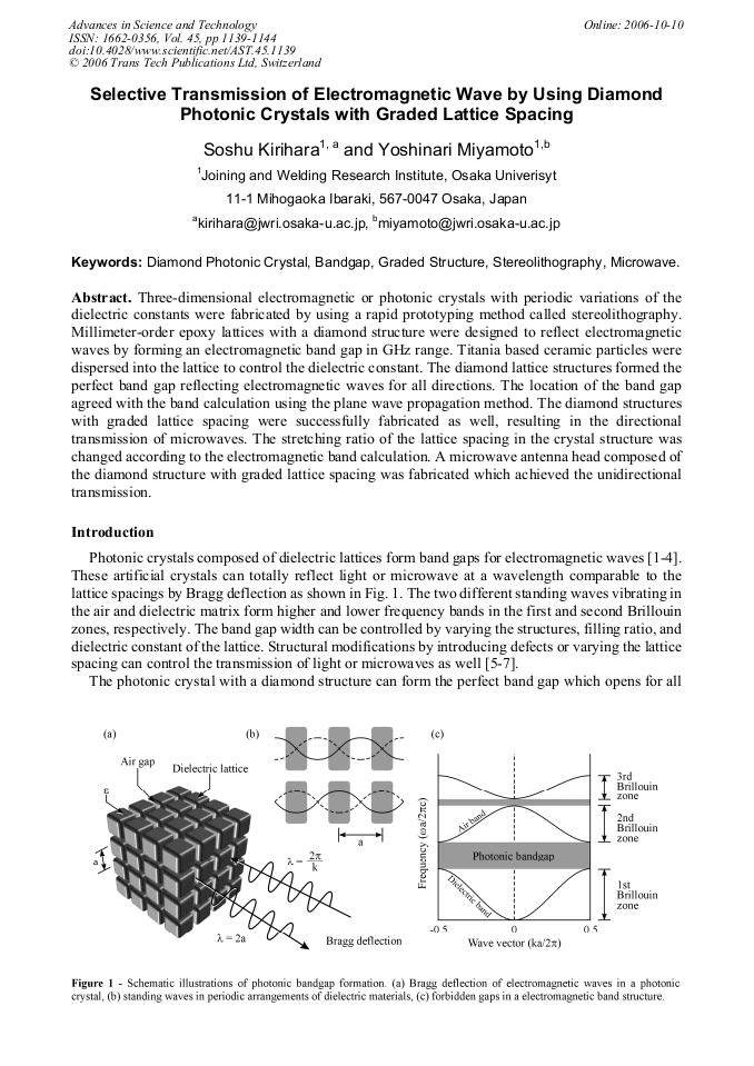
Three-dimensional electromagnetic or photonic crystals with periodic variations of the dielectric constants were fabricated by using a rapid prototyping method called stereolithography. Millimeter-order epoxy lattices with a diamond structure were designed to reflect electromagnetic waves by forming an electromagnetic band gap in GHz range. Titania based ceramic particles were dispersed into the lattice to control the dielectric constant. The diamond lattice structures formed the perfect band gap reflecting electromagnetic waves for all directions. The location of the band gap agreed with the band calculation using the plane wave propagation method. The diamond structures with graded lattice spacing were successfully fabricated as well, resulting in the directional transmission of microwaves. The stretching ratio of the lattice spacing in the crystal structure was changed according to the electromagnetic band calculation. A microwave antenna head composed of the diamond structure with graded lattice spacing was fabricated which achieved the unidirectional transmission.
Info:
Periodical:
Pages:
1139-1144
DOI:
Citation:
Online since:
October 2006
Authors:
Price:
Сopyright:
© 2006 Trans Tech Publications Ltd. All Rights Reserved
Share:
Citation: