p.813
p.819
p.825
p.831
p.837
p.844
p.851
p.857
p.863
Diagram of Electromigration Pattern in Eutectic Pb-Sn and Pb-Free Solders
Abstract:
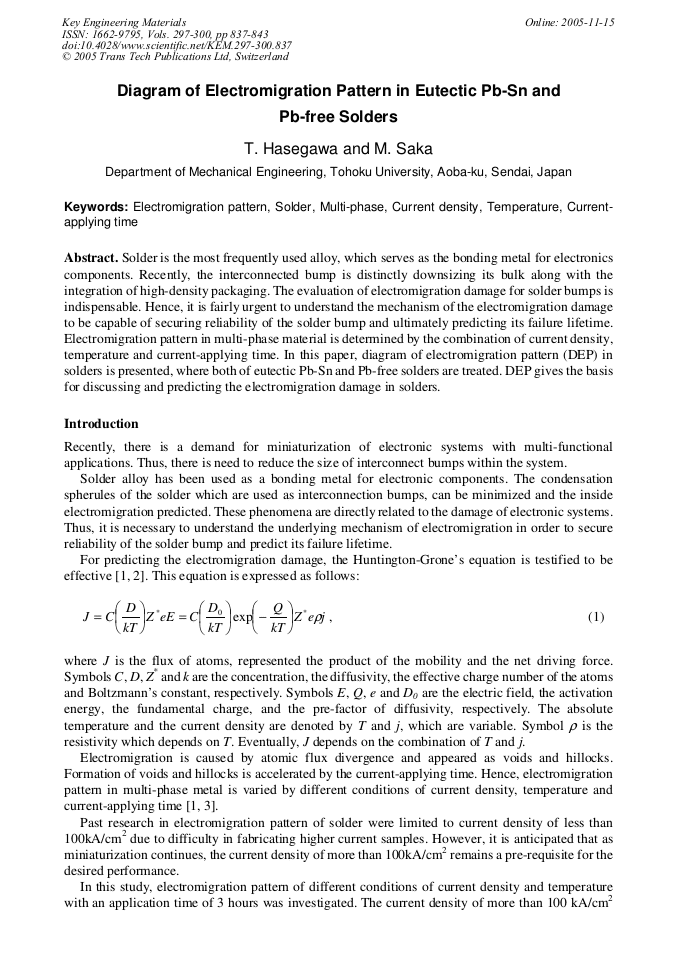
Solder is the most frequently used alloy, which serves as the bonding metal for electronics components. Recently, the interconnected bump is distinctly downsizing its bulk along with the integration of high-density packaging. The evaluation of electromigration damage for solder bumps is indispensable. Hence, it is fairly urgent to understand the mechanism of the electromigration damage to be capable of securing reliability of the solder bump and ultimately predicting its failure lifetime. Electromigration pattern in multi-phase material is determined by the combination of current density, temperature and current-applying time. In this paper, diagram of electromigration pattern (DEP) in solders is presented, where both of eutectic Pb-Sn and Pb-free solders are treated. DEP gives the basis for discussing and predicting the electromigration damage in solders.
Info:
Periodical:
Pages:
837-843
Citation:
Online since:
November 2005
Authors:
Price:
Сopyright:
© 2005 Trans Tech Publications Ltd. All Rights Reserved
Share:
Citation:


