Field Emission Behavior of the Transferred Substrate Aligned Array Carbon Nanotube Films

Article Preview

Abstract:

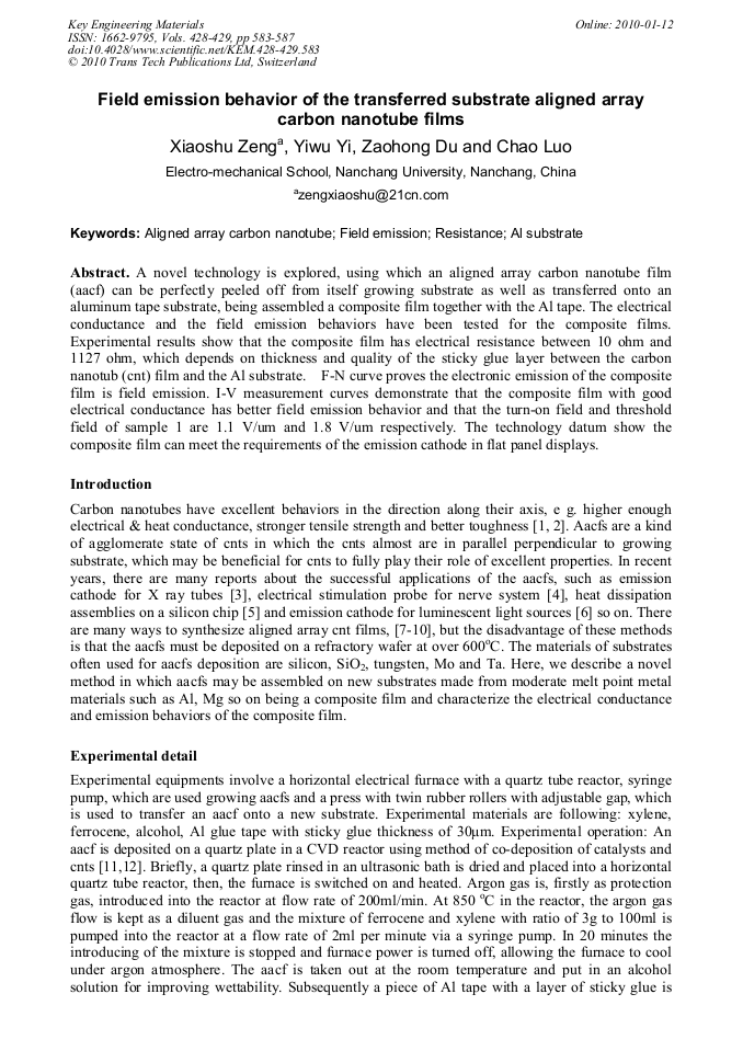
A novel technology is explored, using which an aligned array carbon nanotube film (aacf) can be perfectly peeled off from itself growing substrate as well as transferred onto an aluminum tape substrate, being assembled a composite film together with the Al tape. The electrical conductance and the field emission behaviors have been tested for the composite films. Experimental results show that the composite film has electrical resistance between 10 ohm and 1127 ohm, which depends on thickness and quality of the sticky glue layer between the carbon nanotub (cnt) film and the Al substrate. F-N curve proves the electronic emission of the composite film is field emission. I-V measurement curves demonstrate that the composite film with good electrical conductance has better field emission behavior and that the turn-on field and threshold field of sample 1 are 1.1 V/um and 1.8 V/um respectively. The technology datum show the composite film can meet the requirements of the emission cathode in flat panel displays.

You might also be interested in these eBooks

Info:

Periodical:

Key Engineering Materials (Volumes 428-429)

Pages:

583-587

Citation:

Online since:

January 2010

Export:

Price:

Permissions CCC:

Permissions PLS:

Сopyright:

© 2010 Trans Tech Publications Ltd. All Rights Reserved

Share:

Citation:

[1] W. Z. Li, S. S. Xie, L. X. Qian et al. Science Vol. 274 (1996), p.1701.

Google Scholar

[2] D. Sarangi, I. Arfaoui, A. Chatelain et al. Tsukuba Symposium on Carbon Nannotube in Commenoration of the 10th Anniversary of its Discovery p.24.

Google Scholar

[3] A. Haga et al, Appl. Phys. Lett. Vol. 84 (2004), p.2208.

Google Scholar

[4] M. Andrea, G. Michele, C. Stephane et al. The Journal of Neuroscience Vol. 27 (2007), p.6931.

Google Scholar

[5] K. Kordás, G. Tóth, P. Moilanen, M. Kumpumäki, J. Vähäkangas, and A. Uusimäki: Appl. Phys. Lett. Vol. 90 (2007), p.1247.

DOI: 10.1063/1.2714281

Google Scholar

[6] J. M Bonard, M. Croci, O. Noury et al. Tsukuba Symposium on Carbon Nannotube in Commemoration of the 10th Anniversary of its Discovery (2003), p.32.

Google Scholar

[7] W. Z. Li, S. S. Xie, L. X. Qian et al. Science Vol. 274 (1996), p.1701.

Google Scholar

[8] Z. F. Ren, Z. P. Huang, J. W. Xu et al. Science Vol. 282 (1998), p.1105.

Google Scholar

[9] M. Terrones, M. Grobert, N. Zhang et al. Chem. Phys. Lett Vol. 285 (1998), p.299.

Google Scholar

[10] S. S. Huan, M. G. Chapline, N. R. Franklin et al. Science vol. 283 (1999), p.512.

Google Scholar

[11] X. Zeng, D. Cao, Z. Zhou et al. Journal of Synthetic Crystals, Vol. 32 (2003), p.175.

Google Scholar

[12] X. Zeng and X. Fu: Chinese Journal of Liquid Crystals and Displays Vol. 20 (2005), p.173.

Google Scholar

[13] X. Zeng, China patent, State intellectural property Office of P.R. C, Patent No. ZL03103078. 5.

Google Scholar

[14] J. M. Bonard, M. F. Stockli et al. Ultramicroscopy Vol. 73 (1998), p.7.

Google Scholar

[15] X. Xu and G. R. Brandes: Appl. Phys. Lett. Vol. 74 (1999), p.2549.

Google Scholar

[16] O. M. Küttel, O. Grōning, C. Emmenegger et al: Appl Phys Lett , Vol. 37 (1998), p.2113.

Google Scholar

[17] W. Zhu, C. Bower, O. Zhou et al: Appl. Phys. Lett. Vol. 75 (1999), p.873.

Google Scholar

[18] A. M. Rao, D. Jacques, R. C. Haddon et al: J. Appl. Phys. Vol. 76 (2000), p.3813.

Google Scholar

[19] O. Grōning, O. M. Küttel, C. Emmenegger et al: J. Vac. Sci. Technol, Vol. B18 (2000, p.665.

Google Scholar

[20] J. L. Kwo, C. C. Tsou , M. Yokoyama et al: J Vac. Sci. Technol Vol. B19 (2001), p.23.

Google Scholar

[21] T. R. Cho, J. H. Lee, Y. H. Song et al: Mater Sci. Eng. Vol. B79 (2001), p.128.

Google Scholar