Recent Progress on Controlled Dielectrophoretic Assembly of Carbon Nanotubes

Article Preview

Abstract:

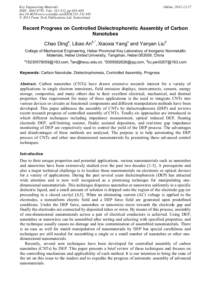
Carbon nanotubes (CNTs) have drawn extensive research interest for a variety of applications in single electron transistors, field emission displays, interconnects, sensors, energy storage, composites, and many others due to their excellent electrical, mechanical, and thermal properties. One requirement for many of these applications is the need to integrate CNTs into various devices or circuits as functional components and different manipulation methods have been developed. This paper addresses the assembly of CNTs by dielectrophoresis (DEP) and reviews recent research progress of controlled assembly of CNTs. Totally six approaches are introduced in which different techniques including impedance measurement, optical induced DEP, floating electrode DEP, self-limiting resistor, fluidic assisted deposition, and real-time gap impedance monitoring of DEP are respectively used to control the yield of the DEP process. The advantages and disadvantages of these methods are analysed. The purpose is to help automating the DEP process of CNTs and other one-dimensional nanomaterials by presenting these advanced control techniques.

You might also be interested in these eBooks

Info:

Periodical:

Key Engineering Materials (Volumes 531-532)

Pages:

485-489

Citation:

Online since:

December 2012

Export:

Price:

Permissions CCC:

Permissions PLS:

Сopyright:

© 2013 Trans Tech Publications Ltd. All Rights Reserved

Share:

Citation:

[1] P. Avouris: Chem. Phys. Vol. 281 (2002), p.429

Google Scholar

[2] J.U. Lee: Appl. Phys. Lett. Vol. 87 (2005), p.073101

Google Scholar

[3] R.J. Chen, et al.: P. Natl. Acad. Sci. USA Vol. 100 (2003), p.4984

Google Scholar

[4] H.W. Seo, C.S. Han, W.S. Jang and J. Park: Curr. Appl. Phys. Vol. 6S1 (2006), p. e216

Google Scholar

[5] Y. Lu, C. Chen, L. Yang and Y. Zhang: Nanoscale Res. Lett. Vol. 4 (2009), p.157

Google Scholar

[6] J. Suehiro, G. Zhou and M. Hara: J. Phys. D: Appl. Phys. Vol. 36 (2003), p. L109

Google Scholar

[7] J. Suehiro, N. Ikeda, A. Ohtsubo, K. Imasaka: Microfluid. Nanofluid. Vol. 5 (2008), p.741

Google Scholar

[8] R. Hamada, et al.: J. Phys.: Conf. Ser. Vol. 307 (2011), p.012031

Google Scholar

[9] M.W. Lee, Y.H. Lin and G.B. Lee: Microfluid. Nanofluid. Vol. 8 (2010), p.609

Google Scholar

[10] P.F. Wu and G.B. Lee: Advances in OptoElectronics Vol. 2011 (2011), p.4827411

Google Scholar

[11] P.J. Pauzauskie, A. Jamshidi, J.K. Valley, J.H. Satcher and M.C. Wu: Appl. Phys. Lett. Vol. 95 (2009), p.113104

Google Scholar

[12] S. Golan, D. Elata and U. Dinnar: Sensor. Actuat. A-Phys. Vol.142 (2008), p.138

Google Scholar

[13] D. Xu, K. Shou, B.J. Nelson: Microelectron. Eng. Vol.88 (2011), p.2703

Google Scholar

[14] L. Dong et al.: J. Phys. Chem. B Vol. 109 (2005), p.13148

Google Scholar

[15] S. Banerjee, B.E. White, L. Huang, B.J. Rego, S. O'Brien and I.P. Herman: J. Vac. Sci. Technol. B Vol. 24 (2006), p.3173

Google Scholar

[16] A. Arun, P. Salet and A.M. Ionescu: J. Electronic Materials Vol. 38 (2009), p.742

Google Scholar

[17] M. Tan, X. Ye, X. Wang and Z. Zhou: Nanotechnology and Precision Engineering Vol. 8 (2010), p.389

Google Scholar

[18] L. An and C. Friedrich: Appl. Phys. Lett. Vol. 92 (2008), p.173103

Google Scholar

[19] L. An and C. Friedrich: J. Appl. Phys. Vol. 105 (2009), p.074314

Google Scholar

[20] L. An, D. Cheam and C. Friedrich: J. Phys. Chem. C. Vol. 113 (2009), p.37

Google Scholar