Research on TSV Dry Etching Technology

Article Preview

Abstract:

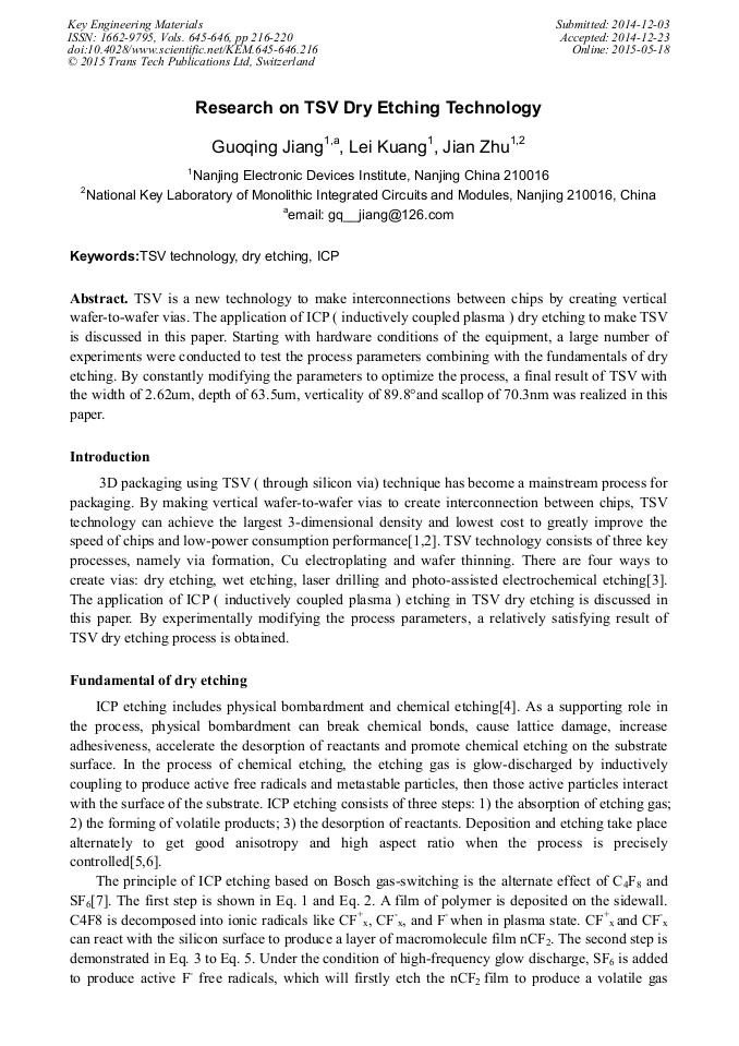
TSV is a new technology to make interconnections between chips by creating vertical wafer-to-wafer vias. The application of ICP ( inductively coupled plasma ) dry etching to make TSV is discussed in this paper. Starting with hardware conditions of the equipment, a large number of experiments were conducted to test the process parameters combining with the fundamentals of dry etching. By constantly modifying the parameters to optimize the process, a final result of TSV with the width of 2.62um, depth of 63.5um, verticality of 89.8°and scallop of 70.3nm was realized in this paper.

You might also be interested in these eBooks

Info:

Periodical:

Key Engineering Materials (Volumes 645-646)

Pages:

216-220

Citation:

Online since:

May 2015

Export:

Price:

Permissions CCC:

Permissions PLS:

Сopyright:

© 2015 Trans Tech Publications Ltd. All Rights Reserved

Share:

Citation:

* - Corresponding Author

[1] Tong Zhiyi, 3D IC Stacking with TSV Interconnect, J. Package and Test. 170(2009) 27-34.

Google Scholar

[2] John H. Lau, Raleigh Convention Center, J. Raleigh-USA. 232(2010) 46-50.

Google Scholar

[3] Huang Bo, TSV Technology Research, J. Scientific Practice. 12(2013)301-302.

Google Scholar

[4] Liao Ke, Wang Zhiyuan, Application of Inductively Coupled Plasma Etching Technique in 808 nm Laser, J. Chinese Materials Science Technology & Equipment. 5(2007) 101-103.

Google Scholar

[5] Chen Shaojun, Li Yigui, Parameter Optimization Based on High-Aspect Ratio Si Dry Etching, J. Micronanoelectronic Technology. 46(2009) 750-754.

Google Scholar

[6] Zhuo Min, Jia Shixing, Zhu Jian, ICP Process in Fabrication of Micro-Inertial Devices, J. Journal of Transduction Technology. 19(2006) 45-47.

Google Scholar

[7] Xu Gaobing, Huang Hua, Zhan Minghao, Huang Xiaoli, et al. Experimental Evaluation of Inductively Coupled Plasma Deep Silicon Etching, J. Journal of Vacuum Science and Technology. 33(2013) 832-835.

Google Scholar