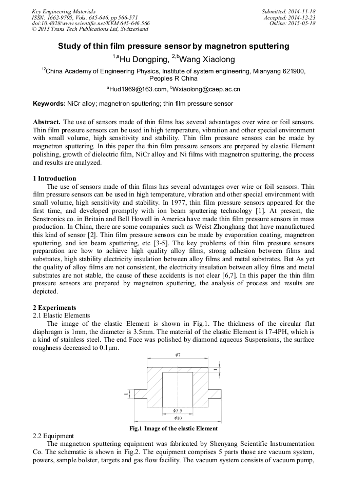
[1]
Chang Zengpo, Tang Baisen. Dynamic characteristics of ion beam sputtered thin-film pressure transducer [J]. Journal of Transducer Technology, 2001, 20(6): 15-17.
Google Scholar
[2]
Li Rong. The current situation and development trend of pressure sensors [J]. Journal of Xian Technological University, 2002, 22(3): 241 -243.
Google Scholar
[3]
Alonso A, Garcia E, Castanl, et al. Strain sensitivity and temperature influence on sputtered thin films for Piezoresistive sensors [J]. Sensors and Actuators A, 1993 37-38: 784-789.
DOI: 10.1016/0924-4247(93)80132-z
Google Scholar
[4]
Angadi M A, Whiting R. Longitudinal and transverse strain sensitivity of nichrome films [J], Mater. Sci. Eng. B, 1990, L1-L4: 7-11.
DOI: 10.1016/0921-5107(90)90020-c
Google Scholar
[5]
Kazi Imam H, Wild P M, Moore T N, et al. The electromechanical behavior of nichrome(80/20wt. %) film [J], Thin Solid Films, 2003, 433: 337-343.
DOI: 10.1016/s0040-6090(03)00390-0
Google Scholar
[6]
Klokhoim E, Berry B S. Intrinsic stress in evaporated metal films [J]. Journal of Elect rochem. Soc., 1968, 115: 823.
Google Scholar
[7]
Qu Xixin, Yang Bangzhao, Jiang Jiejian. Electronic thin film materials [M]. Beijing, Science Press, 1990, 112 -113.
Google Scholar
[8]
He Yinghui,Research on the Performance of thin film pressure sensor and Soft Ware Compensation [D], Changsha: Zhongnan University, 2004.
Google Scholar
[9]
Gong Jianhua, Wang Yating, Jia Qingyun. Discussion on film damage mechanism of large areas of SiO2 thin film deposited by intermediate frequency sputtering [J]. Vacuum, 2003, (4)29-31.
Google Scholar
[10]
Xu Sheng, Hou Xiaobo, Fan Chuizhen. On-line continuous deposition of SiO2 by medium frequency reactive sputtering and ITO by direct current sputtering [J]. Vacuum, 2002, (5): 15-18.
Google Scholar
[11]
Akimori Tabata, Noriaki Matsuno, Yasuo Suzuoki. Optical properties and structure of SiO2 films prepared by ion-beam sputtering [J]. Thin Solid Films, 1996, 289: 84-89.
DOI: 10.1016/s0040-6090(96)08899-2
Google Scholar
[12]
Zhang Jinsong, Ren Zhaoxing, Liang Rongqing. Influence of RF substrate bias on SiO2 films prepared by ECR PECVD [J]. Nuclear Fusion and Plasma Physics,2001, (1)59-64.
Google Scholar
[13]
Jiang Nan, Hugon M C, Agius B, et al. High quality SiO2 films deposited by distributed electron cyclotron resonance plasma enhanced chemical vapor deposition [J]. Vacuum Science and Technology, 1998, (3): 161-169.
DOI: 10.1116/1.579609
Google Scholar
[14]
Markwitz A, Trompetter W J, White G V, et al. Ion microscope investigations of non-uniform surfaces of thin SiO2 films produced by high-temperature nitridation experiments [J], Nuclear Instruments and Methods in Physics Research B, 2001, 181: 354-359.
DOI: 10.1016/s0168-583x(01)00369-x
Google Scholar
[15]
Knoblich B, Gerber T. Aggregation in SiO2 sols from sodium silicate solutions [J], Journal of Non-Crystalline Solids, 2001, 283: 109-113.
DOI: 10.1016/s0022-3093(01)00356-8
Google Scholar
[16]
Wu Guangming Wang Jue, Shen Jun, et al. Effect of experimental conditions on the structure and properties of nano-porous silica films. Chin. Phys. Soc., 2001, (1): 175-18.
Google Scholar
[17]
Wang Zhendong, Miyamoto Iku, electro thermal alloy [M], chemical industry press, 2006, 1-10.
Google Scholar
[18]
Fan Ping. Temperature coefficient of resistivity of metallic films [J], Journal of Shenzhen University, 2000, 17(4): 33-40.
Google Scholar