p.4021
p.4029
p.4035
p.4039
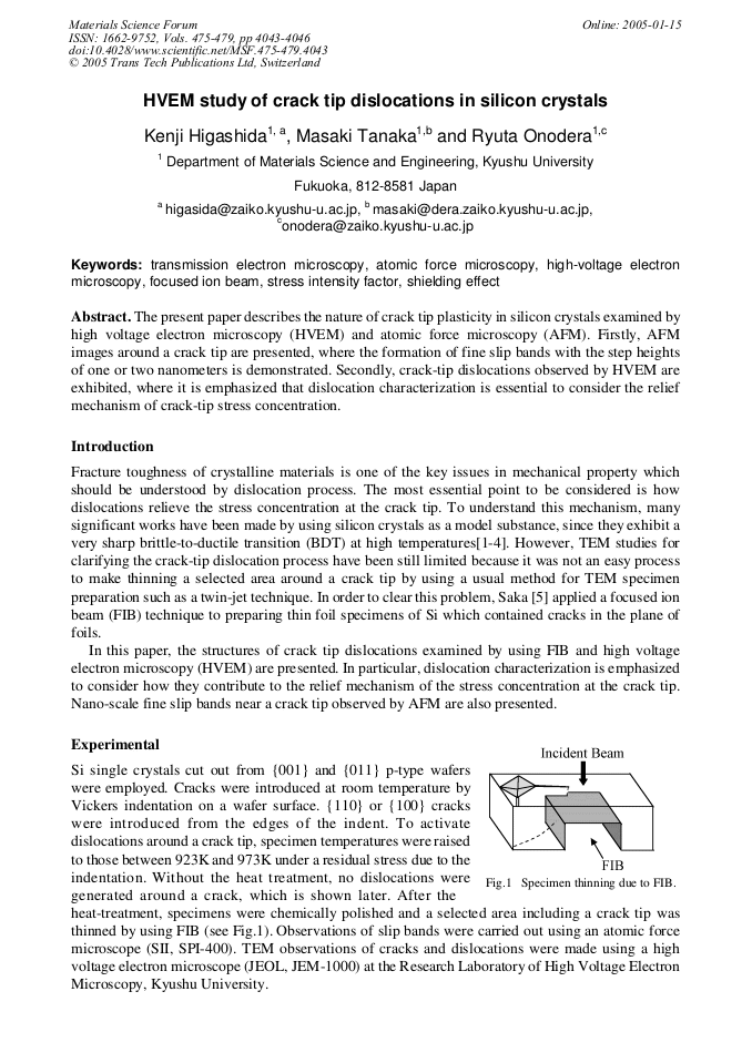
p.4043
p.4047
p.4051
p.4055
p.4059
HVEM Study of Crack Tip Dislocations in Silicon Crystals

Abstract:
The present paper describes the nature of crack tip plasticity in silicon crystals examined by high voltage electron microscopy (HVEM) and atomic force microscopy (AFM). Firstly, AFM images around a crack tip are presented, where the formation of fine slip bands with the step heights of one or two nanometers is demonstrated. Secondly, crack-tip dislocations observed by HVEM are exhibited, where it is emphasized that dislocation characterization is essential to consider the relief mechanism of crack-tip stress concentration.
Info:
Periodical:
Pages:
4043-4046
Citation:
Online since:
January 2005
Authors:
Price:
Сopyright:
© 2005 Trans Tech Publications Ltd. All Rights Reserved
Share:
Citation: