Electrical and Optical Properties of ZnO-Doped Zr0.8Sn0.2TiO4 Thin Films on ITO/Glass Substrates by RF Magnetron Sputtering

Article Preview

Abstract:

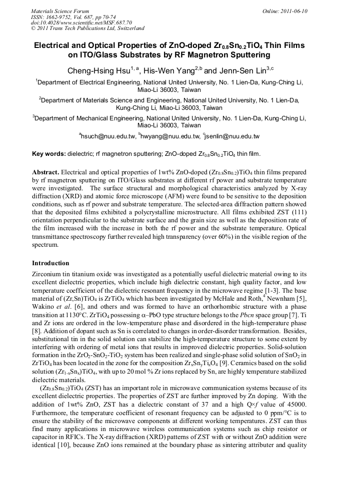
Electrical and optical properties of 1wt% ZnO-doped (Zr0.8Sn0.2)TiO4 thin films prepared by rf magnetron sputtering on ITO/Glass substrates at different rf power and substrate temperature were investigated. The surface structural and morphological characteristics analyzed by X-ray diffraction (XRD) and atomic force microscope (AFM) were found to be sensitive to the deposition conditions, such as rf power and substrate temperature. The selected-area diffraction pattern showed that the deposited films exhibited a polycrystalline microstructure. All films exhibited ZST (111) orientation perpendicular to the substrate surface and the grain size as well as the deposition rate of the film increased with the increase in both the rf power and the substrate temperature. Optical transmittance spectroscopy further revealed high transparency (over 60%) in the visible region of the spectrum.

You might also be interested in these eBooks

Info:

Periodical:

Pages:

70-74

Citation:

Online since:

June 2011

Export:

Price:

Permissions CCC:

Permissions PLS:

Сopyright:

© 2011 Trans Tech Publications Ltd. All Rights Reserved

Share:

Citation:

[1] Y.C. Heiao, L. Wu and C.C. Wei: Mat. Res. Bull. Vol. 23 (1988), p.1687.

Google Scholar

[2] S.I. Hirano, T. Hayashi and A. Hattori: J. Am. Ceram. Soc. Vol. 74 (1991), p.1320.

Google Scholar

[3] H. Tamura, J. Hattori, T. Nishikawa and K. Wakino: Jpn. J. Appl. Phys. Vol. 28 (1989), p.2528.

Google Scholar

[4] A.E. Mchale and R.S. Roth: J. Am. Ceram. Soc. Vol. 69 (1986), p.827.

Google Scholar

[5] R.E. Newnham: J. Am. Ceram. Soc. Vol. 55 (1967), p.409.

Google Scholar

[6] K. Wakino, K. Minai and H. Tamura: J. Am. Ceram. Soc. Vol. 67 (1984), p.278.

Google Scholar

[7] A.E. Mchale and R.S. Roth, J. Am. Ceram. Soc: (1983), p. C-18.

Google Scholar

[8] H. Ikawa, H. Shimojima, K. Urabe, T. Yamada and S. Udagawa: Sci. Ceram. Vol. 14(1987), p.509.

Google Scholar

[9] G. Wolfram and H.E. Goebel: Mater. Res. Bull. Vol. 16 (1981), p.1455.

Google Scholar

[10] C.L. Huang, C.C. You, C.C. Wei and B.C. Shen: J. Wave-Material Interaction Vol. 10 (1995), p.1.

Google Scholar

[11] F.J. Wu and T.Y. Tseng: J. Am. Ceram. Soc. Vol. 81 (1998), p.439.

Google Scholar

[12] O. Nakagawara, Y. Toyota, M. Kobayashi, Y. Yoshino and Y. Katayama: J. Appl. Phys. Vol. 80 (1996), p.388.

Google Scholar

[13] R.B. Dover, L.F. Schneemeyer: IEEE. Elec. Dev. Lett. Vol. 19 (1998), p.329.

Google Scholar

[14] C.L. Huang and C.S. Hsu: J. Vac. Soc. Technol. A Vol. 18 (2000), p.2327.

Google Scholar

[15] B.A. Movchan and A.V. Demshishin: Phys. Met. Metallogr. Vol. 28 (1969), p.83.

Google Scholar

[16] J. A. Thornton: J. Vac. Sci. Technol. A vol. 4 (1986), p.3059.

Google Scholar