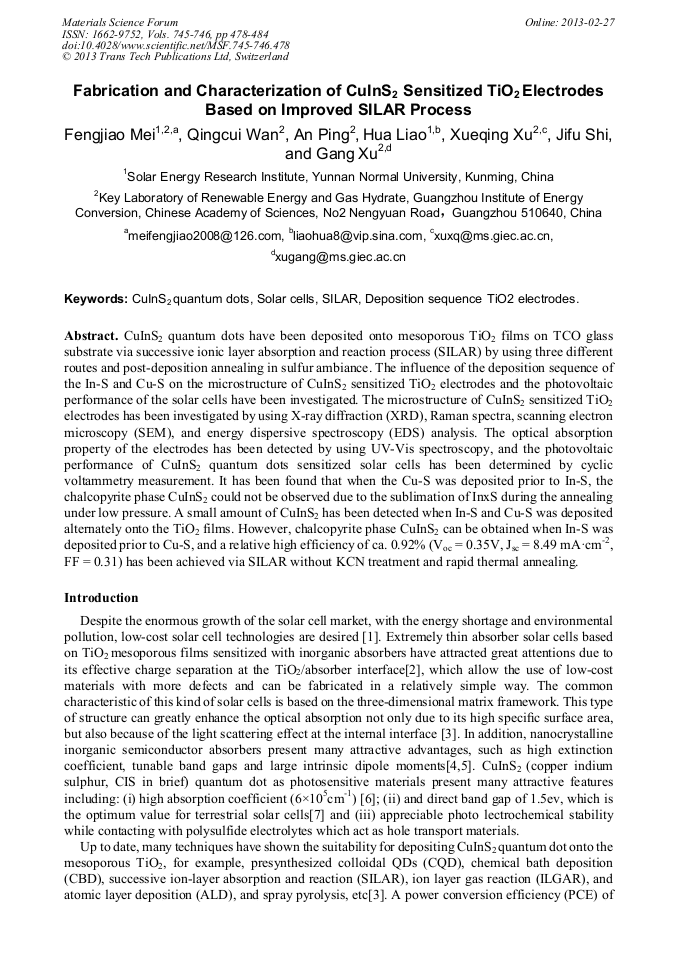
Fabrication and Characterization of CuInS2 Sensitized TiO2 Electrodes Based on Improved SILAR Process

Article Preview

Abstract:

CuInS2 quantum dots have been deposited onto mesoporous TiO2 films on TCO glass substrate via successive ionic layer absorption and reaction process (SILAR) by using three different routes and post-deposition annealing in sulfur ambiance. The influence of the deposition sequence of the In-S and Cu-S on the microstructure of CuInS2 sensitized TiO2 electrodes and the photovoltaic performance of the solar cells have been investigated. The microstructure of CuInS2 sensitized TiO2 electrodes has been investigated by using X-ray diffraction (XRD), Raman spectra, scanning electron microscopy (SEM), and energy dispersive spectroscopy (EDS) analysis. The optical absorption property of the electrodes has been detected by using UV-Vis spectroscopy, and the photovoltaic performance of CuInS2 quantum dots sensitized solar cells has been determined by cyclic voltammetry measurement. It has been found that when the Cu-S was deposited prior to In-S, the chalcopyrite phase CuInS2 could not be observed due to the sublimation of InxS during the annealing under low pressure. A small amount of CuInS2 has been detected when In-S and Cu-S was deposited alternately onto the TiO2 films. However, chalcopyrite phase CuInS2 can be obtained when In-S was deposited prior to Cu-S, and a relative high efficiency of ca. 0.92% (Voc = 0.35V, Jsc = 8.49 mA·cm-2, FF = 0.31) has been achieved via SILAR without KCN treatment and rapid thermal annealing.

You might also be interested in these eBooks

Info:

Periodical:

Materials Science Forum (Volumes 745-746)

Pages:

478-484

Citation:

Online since:

February 2013

Export:

Price:

Permissions CCC:

Permissions PLS:

Сopyright:

© 2013 Trans Tech Publications Ltd. All Rights Reserved

Share:

Citation:

[1] G. Albert, H. Joris, Spray-deposited CuInS2 solar cells, Nanotechnology. 19 (2008) 424018: 1-8.

Google Scholar

[2] T. Dittrich, A. Belaidi, A. Ennaoui, Concepts of inorganic solid-state nanostructured solar cells, Solar Energy Materials and Solar Cells. 95(2011)1527-1536.

DOI: 10.1016/j.solmat.2010.12.034

Google Scholar

[3] Y. Liangliang , Y. Changhui, Review of Quantum Dot Deposition for Extremely Thin Absorber, Solar Cells Science of Advanced Materials. 3(2011)41–58.

DOI: 10.1166/sam.2011.1139

Google Scholar

[4] P.V. Kamat, Quantum Dot Solar Cells: Semiconductor Nanocrystals as Light Harvesters, The Journal of Physical Chemistry C. 112(2008)18737-18753.

DOI: 10.1021/jp806791s

Google Scholar

[5] W.W. Yu, L. Qu, W. Guo, X. Peng, Experimental determination of the extinction coefficient of CdTe, CdSe, and CdS nanocrystals, Chemistry of Materials. 15(2003)2854-2860.

DOI: 10.1021/cm034081k

Google Scholar

[6] S. Siebentritt, Wide gap chalcopyrites: material properties and solar cells, Thin Solid Films. 403-404(2002)1-8.

DOI: 10.1016/s0040-6090(01)01525-5

Google Scholar

[7] M. Green, Solar cells: Operating principles, technology, and system applications, Solar Cells, Prentice-Hall, Englewood Cliffs, (1982).

Google Scholar

[8] T-L. Li, Y-L. Lee, H. Teng, High-performance quantum dot-sensitized solar cells based on sensitization with CuInS2 quantum dots/CdS heterostructure, Energy & Environmental Science. 5(2012)5315-5324.

DOI: 10.1039/c1ee02253a

Google Scholar

[9] J. Feng, J. Han, X. Zhao, Synthesis of CuInS2 quantum dots on TiO2 porous films by solvothermal method for absorption layer of solar cells, Progress in Organic Coatings. 64(2009)268-273.

DOI: 10.1016/j.porgcoat.2008.08.022

Google Scholar

[10] M. Nanu, J. Schoonman, A. Goossens, Solar‐Energy Conversion in TiO2/CuInS2 Nanocomposites, Advanced Functional Materials. 15(2005)95-100.

DOI: 10.1002/adfm.200400150

Google Scholar

[11] M. Nanu, J. Schoonman, A. Goossens, Nanocomposite three-dimensional solar cells obtained by chemical spray deposition, Nano letters. 5(2005)1716-1719.

DOI: 10.1021/nl0509632

Google Scholar

[12] Y.F. Nicolau, Solution deposition of thin solid compound films by a successive ionic-layer adsorption and reaction process, Appl. Surf. Sci. 22/23(1985)1061-1074.

DOI: 10.1016/0378-5963(85)90241-7

Google Scholar

[13] G. Hodes, Chemical Solution Deposition of Semiconductor Films, New York: Marcel Dekker, (2003).

Google Scholar

[14] S. Yong, J. Zhengguo , L. Chunyan, A. Hesong, Q. Jijun, Effect of [Cu]/[In] ratio on properties of CuInS2 thin films prepared by successive ionic layer absorption and reaction method, Applied Surface Science. 252(2006)3737–3743.

DOI: 10.1016/j.apsusc.2005.05.055

Google Scholar

[15] J.J. Wu, W.T. Jiang, W.P. Liao, CuInS2 nanotube array on indium tin oxide: synthesis and photoelectrochemical properties, Chemical Communications. 46(2010)5885-5887.

DOI: 10.1039/c0cc01314e

Google Scholar

[16] H.Y. Chang, W.J. Tzeng, C.H. Lin, S.Y. Cheng, Ionic compounds lamination reaction and characteristics of photosensitive copper indium sulfide on titania nanotube arrays, Journal of Alloys and Compounds. 509(2011)8700-8706.

DOI: 10.1016/j.jallcom.2011.06.018

Google Scholar

[17] I. Oja, M. Nanu, A. Katerski, M. Krunks, A. Mere, J. Raudoja, Goossens A, Crystal quality studies of CuInS2 films prepared by spray pyrolysis, Thin Solid Films. 480(2004)82-86.

DOI: 10.1016/j.tsf.2004.11.013

Google Scholar