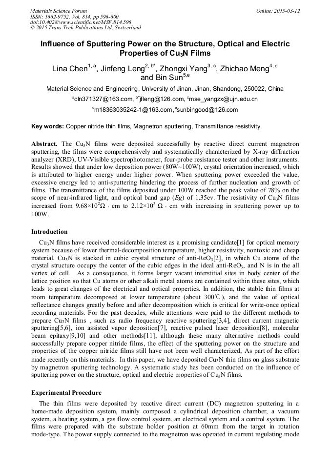
Influence of Sputtering Power on the Structure, Optical and Electric Properties of Cu3N Films

Article Preview

Abstract:

The Cu3N films were deposited successfully by reactive direct current magnetron sputtering, the films were comprehensively and systematically characterized by X-ray diffraction analyzer (XRD), UV-Visible spectrophotometer, four-probe resistance tester and other instruments. Results showed that under low deposition power (80W~100W), crystal orientation increased, which is attributed to higher energy under higher power. When sputtering power exceeded the value, excessive energy led to anti-sputtering hindering the process of further nucleation and growth of films. The transmittance of the films deposited under 100W reached the peak value of 78% on the scope of near-infrared light, and optical band gap (Eg) of 1.35ev. The resistivity of Cu3N films increased from 9.68×10²Ω.cm to 2.12×10³ Ω.cm with increasing in sputtering power up to 100W.

You might also be interested in these eBooks

Info:

Periodical:

Pages:

596-600

Citation:

Online since:

March 2015

Export:

Price:

Permissions CCC:

Permissions PLS:

Сopyright:

© 2015 Trans Tech Publications Ltd. All Rights Reserved

Share:

Citation:

* - Corresponding Author

[1] M. Asano, K. Umeda, A. TasaKi, Jpn.J. Appl. Phys. 29(1990) (1985).

Google Scholar

[2] Z.G. Ji, Y.H. Zhang, Y. Yuan, C. Wang, Mater. Lett. 60 (2006) 3758.

Google Scholar

[3] Z.Q. Liu, W.J. Wang, T.M. Wang, S. Chao, S.K. Zheng, Thin Solid Films. 325 (1998) 55.

Google Scholar

[4] J. Wang, J.T. Chen, X.M. Yuan, Z.G. Wu, B.B. Miao, P.X. Yan, J. Cryst. Growth 286 (2006) 407.

Google Scholar

[5] L. Maya,J. Vac. Sci. Technol. A 11 (1993) 603.

Google Scholar

[6] K.J. Kim, J.H. Kim, J.H. Kang, J. Crystal Growth 222(2001) 767.

Google Scholar

[7] M. Asano, K. Umeda, A. Tasaki, Jpn. J, Appl. Phys. 29 (1990) (1985).

Google Scholar

[8] G. Soto, J.A. Dı´az, W. de la Cruz, Mater. Lett. 57 (2003) 4130.

Google Scholar

[9] D.M. Borsa, D.O. Boerma, Surface Science. 548 (2004) 95.

Google Scholar

[10] Terada S, Tanaka H, Kubota K. Heteroepitaxial growth of Cu3N thin films. Journal of Crystal Growth 1998; 94(2): 567-8.

DOI: 10.1016/0022-0248(89)90038-9

Google Scholar

[11] F. Fendrych, L. Soukup, L. Jastraby´k, M. Sy´ cha, Z. Hubicka, D. Chvostova, A. Tarasenko, V. Studnicka, T. Wagner, Diamond Relat. Mater. 8 (1999) 1715.

Google Scholar

[12] J. Tauc, Grigorovici R, Vancu A. Phys. State. 15(1966) 627.

Google Scholar