p.1025
p.1029
p.1033
p.1037
p.1041
p.1045
p.1049
p.1053
p.1057
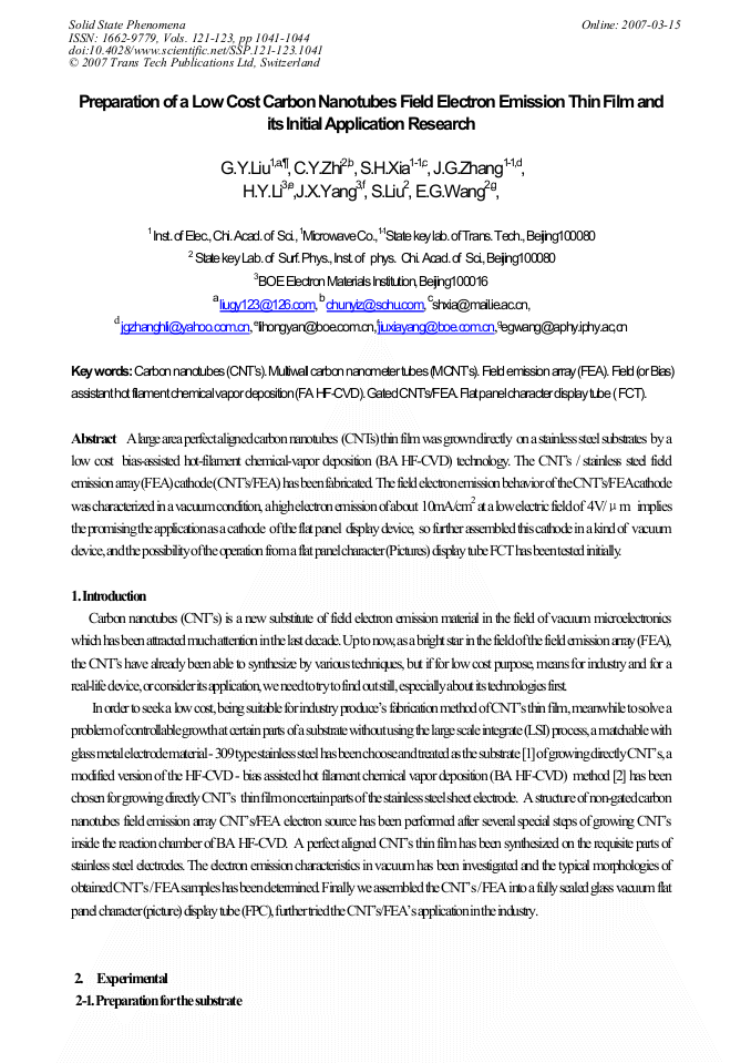
Preparation of a Low Cost Carbon Nanotubes Field Electron Emission Thin Film and its Initial Application Research
Abstract:
A large area perfect aligned carbon nanotubes (CNTs) thin film was grown directly on a stainless steel substrates by a low cost bias-assisted hot-filament chemical-vapor deposition (BA HF-CVD) technology. The CNT’s / stainless steel field emission array (FEA) cathode (CNT’s/FEA) has been fabricated. The field electron emission behavior of the CNT’s/FEA cathode was characterized in a vacuum condition, a high electron emission of about 10mA/cm2 at a low electric field of 4V/μm implies the promising the application as a cathode of the flat panel display device, so further assembled this cathode in a kind of vacuum device, and the possibility of the operation from a flat panel character (Pictures) display tube FCT has been tested initially.
Info:
Periodical:
Pages:
1041-1044
Citation:
Online since:
March 2007
Authors:
Price:
Сopyright:
© 2007 Trans Tech Publications Ltd. All Rights Reserved
Share:
Citation:


