Design of a Rail-to-Rail Operational Amplifier with Low Supply Voltage and Low Power Dissipation
p.3275
p.3275
Design of a 6502-Compatibable Microprocessor
p.3279
p.3279
Design of a Low-Voltage Low-Power CMOS Operational Amplifier
p.3283
p.3283
A Full Integrated LNA in 0.18μm SiGe BiCMOS Technology
p.3287
p.3287
Based on FPGA Design and Simulation of Function Signal Generator
p.3292
p.3292
Design and Implementation of Intelligent Digital Photo Frame Based on FPGA
p.3296
p.3296
Design and Simulation of Photoelectric Detection Circuit for Microfluidics Chip
p.3300
p.3300
Design of a Low-Power Rail-to-Rail CMOS Operational Amplifier
p.3304
p.3304
Design of Pre-Amplifiers for Photoelectric Detector
p.3308
p.3308
Based on FPGA Design and Simulation of Function Signal Generator

Abstract:
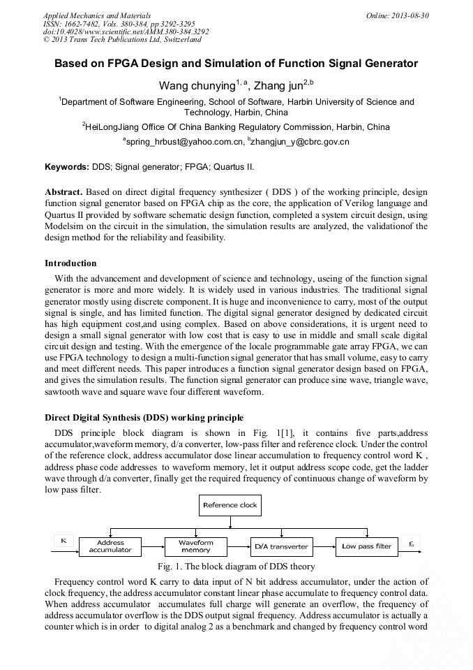
Based on direct digital frequency synthesizer ( DDS ) of the working principle, designfunction signal generator based on FPGA chip as the core, the application of Verilog language andQuartus II provided by software schematic design function, completed a system circuit design, using Modelsim on the circuit in the simulation, the simulation results are analyzed, the validationof the design method for the reliability and feasibility.
You might also be interested in these eBooks
Info:
Periodical:
Applied Mechanics and Materials (Volumes 380-384)
Pages:
3292-3295
Citation:
Online since:
August 2013
Authors:
Price:
Сopyright:
© 2013 Trans Tech Publications Ltd. All Rights Reserved
Share:
Citation: