p.3279
p.3283
p.3287
p.3292
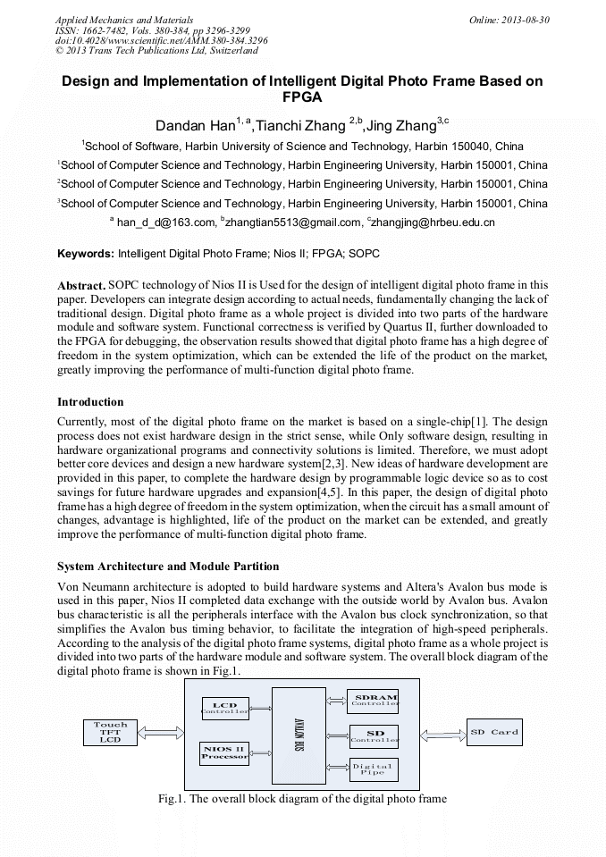
p.3296
p.3300
p.3304
p.3308
p.3312
Design and Implementation of Intelligent Digital Photo Frame Based on FPGA

Abstract:
SOPC technology of Nios II is Used for the design of intelligent digital photo frame in this paper. Developers can integrate design according to actual needs, fundamentally changing the lack of traditional design. Digital photo frame as a whole project is divided into two parts of the hardware module and software system. Functional correctness is verified by Quartus II, further downloaded to the FPGA for debugging, the observation results showed that digital photo frame has a high degree of freedom in the system optimization, which can be extended the life of the product on the market, greatly improving the performance of multi-function digital photo frame.
Info:
Periodical:
Pages:
3296-3299
Citation:
Online since:
August 2013
Authors:
Price:
Сopyright:
© 2013 Trans Tech Publications Ltd. All Rights Reserved
Share:
Citation: