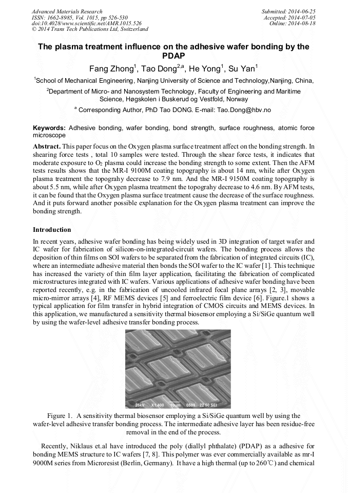
[1]
Monali Joshi, Song Jun Hu, and Mark S. Goorsky, Low Temperature Processing of Porous Silicon Film for Wafer Bonding-Based Thin-Film Layer Transfer Applications, Journal of The Electrochemical Society, Vol. 157, No. 10, pp.909-914, (2010).
DOI: 10.1149/1.3465616
Google Scholar
[2]
Frank Niklaus, Peter Enoksson, Edvard Kälvesten, Göran Stemme, Low temperature full wafer adhesive bonding, Journal of Micromechanics and Microengineering, Vol. 11, No. 2, pp.100-107, (2001).
DOI: 10.1088/0960-1317/11/2/303
Google Scholar
[3]
Zhong, Fang, et al. Low-temperature void-free wafer-level adhesive bonding for thin film transfer by nano-imprint resist., Biomedical Engineering and Informatics (BMEI), 2012 5th International Conference on. IEEE, (2012).
DOI: 10.1109/bmei.2012.6513169
Google Scholar
[4]
Fabian Zimmer, Martin Lapisa, Thor Bakke, Martin Bring, Göran Stemme, One-Megapixel Monocrystalline-Silicon Micromirror Array on CMOS Driving Electronics Manufactured With Very Large-Scale Heterogeneous Integration, Journal of Microelectromechanical Systems, Vol. 20, No. 3, pp.564-572, (2011).
DOI: 10.1109/jmems.2011.2127454
Google Scholar
[5]
Roland Guerre, Ute Drechsler, Debabrata Bhattacharyya, Pekka Rantakari, et al., Wafer-level transfer technologies for PZT-based RF MEMS switches, Journal of Microelectromechanical Systems, Vol. 19, No. 3, pp.548-560, (2010).
DOI: 10.1109/jmems.2010.2047005
Google Scholar
[6]
Jennifer L. Ruglovsky, Young-Bae Park, Cecily A. Ryan, Harry A. Atwater, Wafer bonding and layer transfer for thin film ferroelectrics, MRS Proceedings. Vol. 748. No. 1. Cambridge University Press, (2002).
DOI: 10.1557/proc-748-u11.7
Google Scholar
[7]
Frank Niklaus, Adit Decharat, Fredrik Forsberg, Niclas Roxhed, et al., Wafer bonding with nano-imprint resists as sacrificial adhesive for fabrication of silicon-on-integrated-circuit (SOIC) wafers in 3D integration of MEMS and ICs, Sen. Actu-ators A: Phy., Vol. 154, p.180–186, (2009).
DOI: 10.1016/j.sna.2009.07.009
Google Scholar
[8]
Zhong, F., Dong, T., Yong, H., Yan, S., & Wang, K. (2013). Void-free wafer-level adhesive bonding utilizing modified poly (diallyl phthalate). Journal of Micromechanics and Microengineering, 23(12), 125021.
DOI: 10.1088/0960-1317/23/12/125021
Google Scholar
[9]
Information on http: /www. microresist. de.
Google Scholar
[10]
Frank Niklaus, Göran Stemme, J. Q. Lu, R. J. Gutmann, Adhesive wafer bonding, Journal of Applied Physics, Vol. 99, No. 1, p.031101. 1-031101. 28, (2006).
DOI: 10.1063/1.2168512
Google Scholar
[11]
Harry D Rowland, Amy C Sun, P Randy Schunk, William P King, et al., Impact of polymer film thickness and cavity size on polymer flow during embossing: toward process design rules for nanoimprint lithography, , Journal of Micromechanics and Microengineering, Vol. 15, No. 12, 2414, (2005).
DOI: 10.1088/0960-1317/15/12/025
Google Scholar