p.160
p.166
p.170
p.176
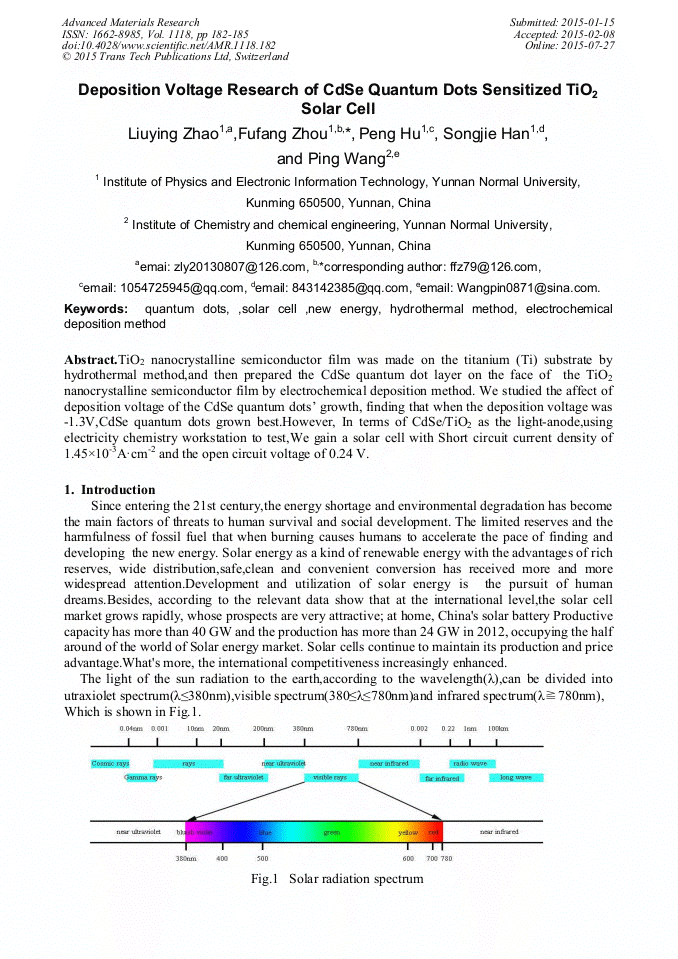
p.182
p.186
p.190
p.195
p.205
Deposition Voltage Research of CdSe Quantum Dots Sensitized TiO2 Solar Cell

Abstract:
TiO2 nanocrystalline semiconductor film was made on the titanium (Ti) substrate by hydrothermal method,and then prepared the CdSe quantum dot layer on the face of the TiO2 nanocrystalline semiconductor film by electrochemical deposition method. We studied the affect of deposition voltage of the CdSe quantum dots’ growth, finding that when the deposition voltage was-1.3V,CdSe quantum dots grown best.However, In terms of CdSe/TiO2 as the light-anode,using electricity chemistry workstation to test,We gain a solar cell with Short circuit current density of 1.45×10⁻³A·cm-2 and the open circuit voltage of 0.24 V.
Info:
Periodical:
Pages:
182-185
DOI:
Citation:
Online since:
July 2015
Authors:
Price:
Сopyright:
© 2015 Trans Tech Publications Ltd. All Rights Reserved
Share:
Citation: