Effects of Annealing Temperature of Indium Tin Oxide Thin Films Prepared onto Glass by Sol-Gel Spin Coating Method

Article Preview

Abstract:

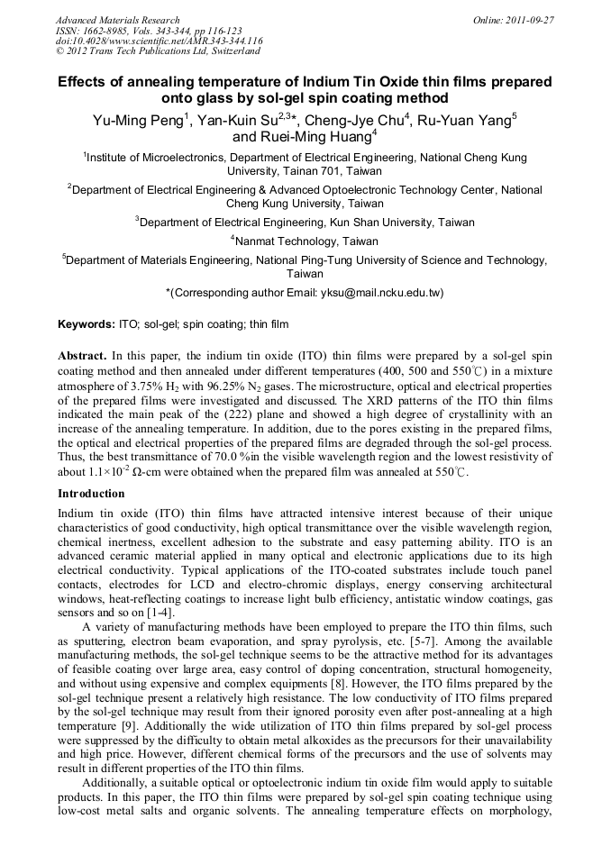
In this paper, the indium tin oxide (ITO) thin films were prepared by a sol-gel spin coating method and then annealed under different temperatures (400, 500 and 550°C) in a mixture atmosphere of 3.75% H2 with 96.25% N2 gases. The microstructure, optical and electrical properties of the prepared films were investigated and discussed. The XRD patterns of the ITO thin films indicated the main peak of the (222) plane and showed a high degree of crystallinity with an increase of the annealing temperature. In addition, due to the pores existing in the prepared films, the optical and electrical properties of the prepared films are degraded through the sol-gel process. Thus, the best transmittance of 70.0 %in the visible wavelength region and the lowest resistivity of about 1.1×10⁻² Ω-cm were obtained when the prepared film was annealed at 550°C.

You might also be interested in these eBooks

Info:

Periodical:

Advanced Materials Research (Volumes 343-344)

Pages:

116-123

Citation:

Online since:

September 2011

Export:

Price:

Permissions CCC:

Permissions PLS:

Сopyright:

© 2012 Trans Tech Publications Ltd. All Rights Reserved

Share:

Citation:

[1] P. K. Manoj, B. Joseph, V. K. Vaidyan and D. S. D. Amma: Ceram. Int. Vol. 33 (2007), pp.273-278.

Google Scholar

[2] R. Pan, S. Qiang, K. Liew, Y. Zhao, R. Wang and J. Zhu: Powder Technol. Vol. 189 (2009), pp.126-129.

Google Scholar

[3] Y. C. Liang: Ceram. Int. Vol. 36 (2010), pp.1743-1747.

Google Scholar

[4] O. Warschkow, D. E. Ellis, G. B. Gonzalez and T. O. Mason: J. Am. Ceram. Soc. Vol. 86 (2003), pp.1700-1706.

Google Scholar

[5] H. C Lee and O. Park: Vacuum Vol. 80 (2006), pp.880-887.

Google Scholar

[6] H. R. Fallah, M. Ghaseni, A. Hassanzadeh and H. Steki: Physica B Vol. 373 (2006), pp.274-279.

Google Scholar

[7] S. M. Rozati and T. Ganj: Renewable Energy Vol. 29 (2004), pp.1671-1676.

Google Scholar

[8] M. Reidinger, M. Rydzek, C. Scherdel, M. Arduini-Schuster and J. Manara: Thin Solid Films Vol. 517 (2009), pp.3096-3099.

DOI: 10.1016/j.tsf.2008.11.078

Google Scholar

[9] A. Solieman and M.A. Aegerter: Thin Solid Films Vol. 502 (2006), pp.205-211.

Google Scholar

[10] L. Yang, X. He and F. He: Materials Letters Vol. 62 (2008), pp.4539-4541.

Google Scholar

[11] B. L. Zhu, X. H. Sun and S. Guo: J. J. Appl. Phys. Vol. 45 (2006), pp.7860-7865.

Google Scholar

[12] Z. H. Li, Y. P. Ke and D. Y. Ren: Trans Nonferrous Met. Soc. China. Vol. 18 (2008), pp.366-371.

Google Scholar

[13] C. Liu, T. Matsutani, T. Asanuma, K. Murai, M. Kiuchi, E. Alves and M. Reis: J. Appl. Phys. Vol. 93 (2003), p.2262.

Google Scholar

[14] J. H. Kim , B. D. Ahn, C. H. Lee, K. A. Jeon, H. S. Kang, G. H. Kim and S. Y. Lee: Thin Solid Films Vol. 515 (2007), pp.3580-3583.

Google Scholar

[15] Y. Gan, J. X. Liu and S. N. Zeng: Surface & Coating Technology Vol. 201 (2006), pp.25-29.

Google Scholar

[16] J. Liu, D. Wu and S. Zeng: J. Mater. Process. Tech. Vol. 209 (2009), pp.3943-3948.

Google Scholar

[17] L. Yang, X. He, D. Ge and H. Wei: Physica B Vol. 404 (2009), pp.2146-2150.

Google Scholar

[18] I. Hambergend and C. G. Granquist: J. Appl. Phys. Vol. 60 (1986), p. R123.

Google Scholar

[19] D. C. Look, J. W. Hemsky and J. R. Sizelove: Phys. Rev. Lett. Vol. 82 (1999), p.2552.

Google Scholar