p.2087
p.2091
p.2099
p.2103
p.2111
p.2116
p.2125
p.2130
p.2134
Influencing Time Response of Nano Photoelectric on the Factors Films
Abstract:
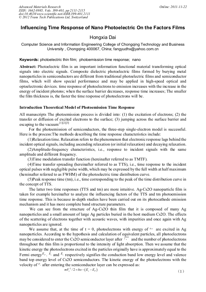
Photoelectric film is an important information functional material transforming optical signals into electric signals. Composite dielectric photoelectric films formed by burying metal nanoparticles in semiconductors are different from traditional photoelectric films and semiconductor films, which will show special performance and may be applied in high-speed optical and optoelectronic devices. time response of photoelectrons to emission increases with the increase in the energy of incident photons; when the surface barrier decreases, response time increases; The smaller the film thickness is, the faster the time response of photoelectrons will be.
Info:
Periodical:
Pages:
2111-2115
Citation:
Online since:
November 2011
Authors:
Keywords:
Price:
Сopyright:
© 2012 Trans Tech Publications Ltd. All Rights Reserved
Share:
Citation:


