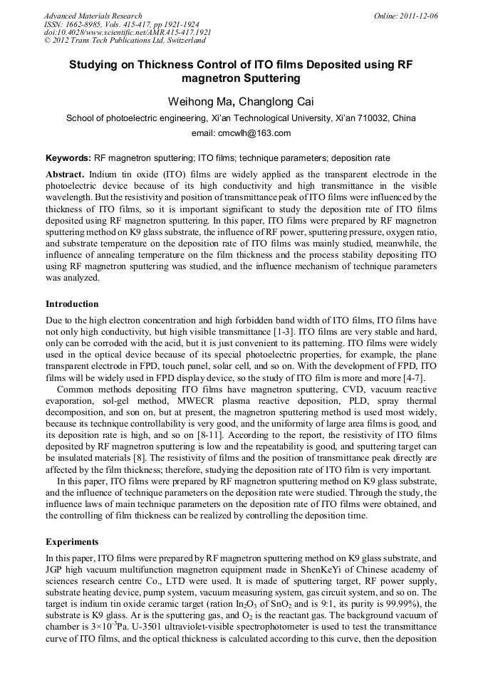
Studying on Thickness Control of ITO Films Deposited Using RF Magnetron Sputtering

Article Preview

Abstract:

Indium tin oxide (ITO) films are widely applied as the transparent electrode in the photoelectric device because of its high conductivity and high transmittance in the visible wavelength. But the resistivity and position of transmittance peak of ITO films were influenced by the thickness of ITO films, so it is important significant to study the deposition rate of ITO films deposited using RF magnetron sputtering. In this paper, ITO films were prepared by RF magnetron sputtering method on K9 glass substrate, the influence of RF power, sputtering pressure, oxygen ratio, and substrate temperature on the deposition rate of ITO films was mainly studied, meanwhile, the influence of annealing temperature on the film thickness and the process stability depositing ITO using RF magnetron sputtering was studied, and the influence mechanism of technique parameters was analyzed.

You might also be interested in these eBooks

Info:

Periodical:

Advanced Materials Research (Volumes 415-417)

Pages:

1921-1924

Citation:

Online since:

December 2011

Export:

Price:

Permissions CCC:

Permissions PLS:

Сopyright:

© 2012 Trans Tech Publications Ltd. All Rights Reserved

Share:

Citation:

[1] H.H. Tao, N. Yao, R.S. Xin, et al: Journal of Zhengzhou University (Natural Science Edition) Vol. 35( 2003), p.37

Google Scholar

[2] R.S. Xin, Y. Lin: Chinese Journal of Rare Metals Vol. 29(2005), p.931

Google Scholar

[3] J.F. Deng, J.J. Li, J.J. Yang: Advanced Display Vol. 58(2005), p.44

Google Scholar

[4] Y.T. Wu, X.L. Weng, L.J. Deng: Chinese Journal of Vacuum Science and Technology Vol. 26(2006), p.372

Google Scholar

[5] X.S. Jiang, C.B. Cao, X.P. Song, et al: Chinese Journal of Liquid Crystals and Displays Vol. 22(2007), p.398

Google Scholar

[6] Z.G. Zhang: Infrared and Laser Engineering Vol. 35(2006), p.200

Google Scholar

[7] J. Wang, H. Lin, G. Yang, et al : Semiconductor Optoelectronics Vol.28(2007), p.68

Google Scholar

[8] X.L. Zhao, B.Y. Ren, L. Zhao, et al: Journal of Optoelectronics laser Vol. 16(2005), p.1429

Google Scholar

[9] S.H. Wang, J.Q. Zhang, B. Wang, et al: Journal of Functional Materials Vol. 40(2009), p.717

Google Scholar

[10] S.R. Zou, H.Y. Wang, M.Y. Geng, et al: Vacuum Vol. 46(2009), p.45

Google Scholar

[11] C.L. Cai, Y.J. Zhai, J. Huang, et al: SPIE Vol.7522(2010), p.75226801

Google Scholar