The Interfacial Characteristics of Ba0.6Sr0.4TiO3 Films Deposited by Radio Frequency Magnetron Sputtering

Article Preview

Abstract:

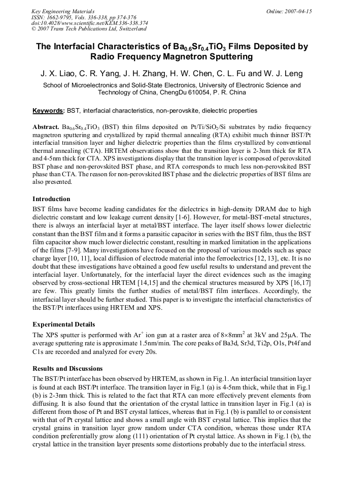
Ba0.6Sr0.4TiO3 (BST) thin films deposited on Pt/Ti/SiO2/Si substrates by radio frequency magnetron sputtering and crystallized by rapid thermal annealing (RTA) exhibit much thinner BST/Pt interfacial transition layer and higher dielectric properties than the films crystallized by conventional thermal annealing (CTA). HRTEM observations show that the transition layer is 2-3nm thick for RTA and 4-5nm thick for CTA. XPS investigations display that the transition layer is composed of perovskited BST phase and non-perovskited BST phase, and RTA corresponds to much less non-perovskited BST phase than CTA. The reason for non-perovskited BST phase and the dielectric properties of BST films are also presented.

You might also be interested in these eBooks

Info:

Periodical:

Key Engineering Materials (Volumes 336-338)

Pages:

374-376

Citation:

Online since:

April 2007

Export:

Price:

Permissions CCC:

Permissions PLS:

Сopyright:

© 2007 Trans Tech Publications Ltd. All Rights Reserved

Share:

Citation:

[1] Lookman, J. McAneney, R. M. Bowman, et al.: J. Appl. Phys. Vol. 85 (2004), p.5010.

Google Scholar

[2] H. W. Wang, S. W. Nien and K. C. Lee: Appl. Phys. Lett. Vol. 84 (2004), p.2874.

Google Scholar

[3] W. Fan, B. Kabius, J. M. Hiller, et al.: J. Appl. Phys. Vol. 94 (2004), p.6192.

Google Scholar

[4] C. Leu, S. H. Chan and H. Y. Chen: Microelectron. Reliab. Vol. 40 (2000), p.679.

Google Scholar

[5] S. Saha and S. B. Krupanidhi: Appl. Phys. Lett. Vol. 79 (2004), p.111.

Google Scholar

[6] J. H. Park, D. H. Hong and Y. B. Kim: J. Appl. Phys. Vol. 91 (2002), p.10022.

Google Scholar

[7] L. J. Sinnamon, R. M. Bowman and J. M. Gregg: Appl. Phys. Lett. Vol. 78 (2001), p.1724.

Google Scholar

[8] L. Goux, M. Gervais and A. Catherinot: Mater. Sci. Semicon. Proc. Vol. 5 (2003), p.189.

Google Scholar

[9] S. Regnery, P. Ehrhart, F. Fitsilis and R. Waser: J. Eur. Ceram. Soc. Vol. 24 (2004), p.271.

Google Scholar

[10] S. Hwang, B. T. Lee, C. S. Kang, et al.: J. Appl. Phys. Vol. 85 (1) (1999), p.287.

Google Scholar

[11] F. M. Pontes, E. R. Leite, E. Longo, et al.: Appl. Phys. Lett. Vol. 76 (17) (2000), p.2433.

Google Scholar

[12] K. Choi, B. S. Kim, S.Y. Son, et al.: J. Appl. Phys. Vol. 86 (6) (1999), p.3347.

Google Scholar

[13] S. H. Oh, K. W. Park, J. H. Park, et al.: J. Vac. Sci. Technol. B Vol. 18 (4) (2000), pp. (1923).

Google Scholar

[14] H. Z. Jin, J. Zhu, P. Ehrhart, et al.: Thin Solid Films, Vol. 429 (2003), p.282.

Google Scholar

[15] C. Yoo and J.Y. Lee: J. Cryst. Growth Vol. 224 (2001), p.251.

Google Scholar

[16] Y. Fujisaki, Y. Shimamoto and Y. Matsui: Jpn. J. Appl. Phys. Vol. 38 (1999), pp. L52.

Google Scholar

[17] V. Craciun and R. K. Singh: Appl. Phys. Lett. Vol. 76 (14) (2000), pp. (1932).

Google Scholar