p.67
p.73
p.79
p.84
p.88
p.92
p.97
p.103
p.108
Crack Behavior of Si-Doped GaAs Crystals Grown by Pulling-Down Method

Abstract:
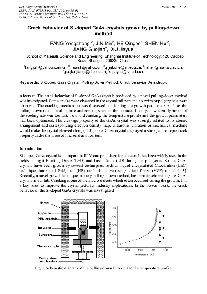
The crack behavior of Si-doped GaAs crystals produced by a novel pulling-down method was investigated. Some cracks were observed in the crystal tail part and no twins or polycrystals were observed. The cracking mechanism was discussed considering the growth parameters, such as the pulling-down rate, annealing time and cooling speed of the furnace. The crystal was easily broken if the cooling rate was too fast. To avoid cracking, the temperature profile and the growth parameters had been optimized. The cleavage property of the GaAs crystal was strongly related to its atomic arrangement and corresponding electron density map. Ultrasonic vibration or mechanical machine would make the crystal cleaved along (110) plane. GaAs crystal displayed a strong anisotropic crack property under the force of microindentation test.
Info:
Periodical:
Pages:
88-91
Citation:
Online since:
December 2012
Authors:
Price:
Сopyright:
© 2013 Trans Tech Publications Ltd. All Rights Reserved
Share:
Citation: