Effect of Substrate Temperature on Crystal Orientation and Residual Stress in RF Sputtered Gallium Nitride Films

Article Preview

Abstract:

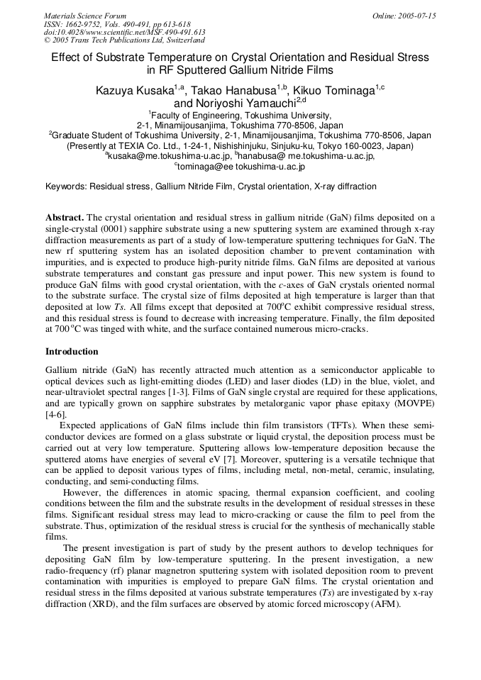
The crystal orientation and residual stress in gallium nitride (GaN) films deposited on a single-crystal (0001) sapphire substrate using a new sputtering system are examined through x-ray diffraction measurements as part of a study of low-temperature sputtering techniques for GaN. The new rf sputtering system has an isolated deposition chamber to prevent contamination with impurities, and is expected to produce high-purity nitride films. GaN films are deposited at various substrate temperatures and constant gas pressure and input power. This new system is found to produce GaN films with good crystal orientation, with the c-axes of GaN crystals oriented normal to the substrate surface. The crystal size of films deposited at high temperature is larger than that deposited at low Ts. All films except that deposited at 700oC exhibit compressive residual stress, and this residual stress is found to decrease with increasing temperature. Finally, the film deposited at 700 oC was tinged with white, and the surface contained numerous micro-cracks.

You might also be interested in these eBooks

Info:

Periodical:

Materials Science Forum (Volumes 490-491)

Pages:

613-618

Citation:

Online since:

July 2005

Export:

Price:

Permissions CCC:

Permissions PLS:

Сopyright:

© 2005 Trans Tech Publications Ltd. All Rights Reserved

Share:

Citation:

[1] S. Nakamura, T. Mukai and M. Senoh, Appl. Phys. Lett., Vol. 64 (1994), p.1687.

Google Scholar

[2] S. Nakamura, M. Senoh, N. Iwasa and S. Nagahama, Jpn. J. Appl. Phys., Vol. 34 (1995), p. L797.

Google Scholar

[3] S. Nakamura, M. Senoh, S. Nagahama, N. Iwasa, T. Yamada, T. Matsushita, H. Kiyohu and, Y. Sugimoto, Jpn. J. Appl. Phys., Vol. 35 (1996), p. L74.

DOI: 10.1143/jjap.35.l74

Google Scholar

[4] S. Miyoshi, K. Onabe, N. Ohkouchi, H. Yaguchi and R. Ito, J. Crystal Growth, Vol. 124 (1992), p.432.

Google Scholar

[5] Y. Kobayashi, F. Scholtz and N. Kobayashi, Jpn. J. Appl. Phys., Vol. 36 (1997), p.2592.

Google Scholar

[6] H. Sato, H. Takahashi, A. Watanabe and H. Ota, Appl. Phys. Lett., Vol. 68 (1996), p.3617.

Google Scholar

[7] R. V. Stuart, G. K. Wehner and G. S. Anderson, J. Appl. Phys., Vol. 40 (1969), p.803.

Google Scholar

[8] T. Hanabusa, Mater. Sci. Res. Int., Vol. 5 (1999), p.63.

Google Scholar

[9] H. P. Maruska and J. J. Tietjen, Appl. Phys. Lett., USA, Vol. 15 (1969), p.327.

Google Scholar

[10] T. Detchprohm, K. Hiramatsu, K. Itoh and I. Akasaki, Jpn. J. Appl. Phys., Vol. 31 (1992), p. L1454.

Google Scholar

[11] E. Macherauch and P. Müller, Z. angew Phys., Vol. 13 (1961), p.305.

Google Scholar

[12] V. A. Savastenko and A. U. Sheleg, Phys. Status Solidi A (Germany), Vol. 48 (1978), p. K135.

Google Scholar

[13] U. Geyer, U. von Hülsen, H. Kopf, J. Appl. Phys., Vol. 83 (1998), p.3065.

Google Scholar

[14] D. W. Hoffman and J. A. Thornton, Thin Solid Films, Vol. 45 (1977), p.387.

Google Scholar

[15] J. A. Thornton and D. W. Hoffman, J. Vac. Sci. & Tech., Vol. A3 (1985), p.576.

Google Scholar

[16] G. Este, R. Surridge and W. D. Westwood, J. Vac. Sci. & Tech., Vol. A4 (1986), p.989.

Google Scholar

[17] G. Este and W. D. Westwood, J. Vac. Sci. & Tech., Vol. A5 (1987), p. (1982).

Google Scholar