Electronic Properties of Cubic Boron Nitride with Impurity Atoms and Vacancy
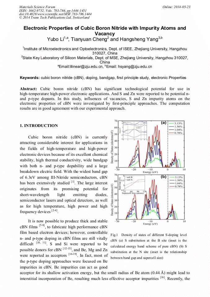
Article Preview

Abstract:

Cubic boron nitride (cBN) has significant technological potential for use in high-temperature high-power electronic applications. And S and Zn were reported to be potential n-and p-type dopants. In this study, influences of vacancies, S and Zn impurity atoms on the electronic properties of cBN were investigated by first-principle approaches. The computation results are in good agreement with our experimental approach.

You might also be interested in these eBooks

Info:

Periodical:

Materials Science Forum (Volumes 783-786)

Pages:

1444-1451

Citation:

Online since:

May 2014

Export:

Price:

Permissions CCC:

Permissions PLS:

Сopyright:

© 2014 Trans Tech Publications Ltd. All Rights Reserved

Share:

Citation:

* - Corresponding Author

[1] N. Miyata, K. Moriki, O. Mishima, M. Fujisawa, T. Hattori, Optical constants of cubic boron nitride, Phys. Rev. B 40 (1989) 12028.

DOI: 10.1103/physrevb.40.12028

Google Scholar

[2] C.H. Lin, C.W. Liu. Metal-Insulator-Semiconductor Photodetectors. Sensors 10 (2010) 8797.

Google Scholar

[3] L.H. Chen, Development of III-V semiconductor FPA photodetectors of full optical spectrum. Infrared and Laser Engineering 37 (2008) 1.

Google Scholar

[4] A. Soltani, H.A. Barkad, M. Mattalah, B. Benbakhti, J.C. De Jaeger, Y.M. Chong, Y.S. Zou, W.J. Zhang, S.T. Lee, A. BenMoussa, B. Giordanengo, J.F. Hochedez, 193 nm deep-ultraviolet solar-blind cubic boron nitride based photodetectors, Appl. Phys. Lett. 92 (2008).

DOI: 10.1063/1.2840178

Google Scholar

[5] S. Matsumoto, Z. Wenjun, Jpn. J. Appl. Phys. 39 (2000) L442.

Google Scholar

[6] W.J. Zhang, I. Bello, Y. Lifshitz, K.M. Chan, Y. Wu, C.Y. Chan, X.M. Meng, S.T. Lee, Appl. Phys. Lett. 85 (2004) 1344.

Google Scholar

[7] H. Boyen, P. Wedmayer, D. Schwertberger, N. Deyneka, P. Ziemann, Appl. Phys. Lett. 76 (2000) 709.

Google Scholar

[8] P. Ziemann, H. Boyen, N. Deyneka, P. Widmayer, D. Schwertberger, Adv. Solid State Phys. 40 (2000) 423.

Google Scholar

[9] H. Yang, A. Chen, F. Qiu, Cubic boron nitride film residual compressive stress relaxation by post annealing, Diamond Relat. Mater. 20 (2011) 1179.

DOI: 10.1016/j.diamond.2011.07.003

Google Scholar

[10] R. H. Wentorf, Jr: J. Chem. Phys. 36 (1962) (1990).

Google Scholar

[11] O. Mishima, K. Era, J. Tanaka and S. Yamoka, Appl. Phys. Lett. 53 (1988) 962.

Google Scholar

[12] J. Ying, X.W. Zhang, Z.G. Yin, H.R. Tan, S.G. Zhang, Y.M. Fan, Electrical transport properties of the Si-doped cubic boron nitride thin films prepared by in situ cosputtering, J. Appl. Phys. 109 (2011) 023716.

DOI: 10.1063/1.3544065

Google Scholar

[13] J. Ying, X.W. Zhang, Z.G. Yin, H.R. Tan, S.G. Zhang, Y.M. Fan, Electrical transport properties of the Si-doped cubic boron nitride thin films prepared by in situ cosputtering, J. Appl. Phys. 109 (2011) 023716.

DOI: 10.1063/1.3544065

Google Scholar

[14] H.S. Yang, N. Kurebayashi, T. Yoshida, In situ S-doping of cubic boron nitride thin films by plasma enhanced chemical vapor deposition, in: T. Chandra, N. Wanderka, W. Reimers, M. Ionescu (Eds. ) (Trans Tech Publ, Berlin, 2010) p.2956.

DOI: 10.4028/www.scientific.net/msf.638-642.2956

Google Scholar

[15] Y.B. Li, H.X. Jiang, G.Z. Yuan, A.L. Chen, X. Wang, T.G. Dai, H.S. Yang, Electronic structure and impurity states of S-doped cBN: A first-principle study, J. Alloy and Compounds 531 (2012) 82.

DOI: 10.1016/j.jallcom.2012.04.002

Google Scholar

[16] B. He, W.J. Zhang, Y.S. Zou, Y.M. Chong, Q. Ye, A.L. Ji, Y. Yang, I. Bello, S.T. Lee, G.H. Chen, Electrical properties of Be-implanted polycrystalline cubic boron nitride films, Appl. Phys. Lett. 92 (2008) 102108.

DOI: 10.1063/1.2896643

Google Scholar

[17] K. Nose, H. Oba, T. Yoshida, Electric conductivity of boron nitride thin films enhanced by in situ doping of zinc, Appl. Phys. Lett. 89 (2006) 112124.

DOI: 10.1063/1.2354009

Google Scholar

[18] K. Nose, T. Yoshida, Semiconducting properties of zinc-doped cubic boron nitride thin films, J. Appl. Phys. 102 (2007) 063711.

DOI: 10.1063/1.2783983

Google Scholar