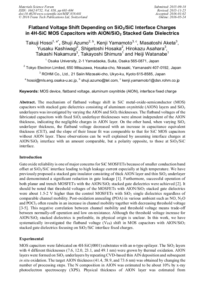
Flatband Voltage Shift Depending on SiO2/SiC Interface Charges in 4H-SiC MOS Capacitors with AlON/SiO2 Stacked Gate Dielectrics

Article Preview

Abstract:

The mechanism of flatband voltage shift in SiC metal-oxide-semiconductor (MOS) capacitors with stacked gate dielectrics consisting of aluminum oxynitride (AlON) layers and SiO2 underlayers was investigated by varying the AlON and SiO2 thicknesses. The flatband voltages of the fabricated capacitors with fixed SiO2 underlayer thicknesses were almost independent of the AlON thickness, indicating the negligible charges in AlON layer. On the other hand, when varying SiO2 underlayer thickness, the flatband voltage decreased with an increase in capacitance equivalent thickness (CET), and the slope of their linear fit was comparable to that for SiC MOS capacitors without AlON layer. These observations can be well explained by assuming interface charges at AlON/SiO2 interface with an amount comparable, but a polarity opposite to, those at SiO2/SiC interface.

You might also be interested in these eBooks

Info:

Periodical:

Pages:

681-684

Citation:

Online since:

May 2016

Export:

Price:

Permissions CCC:

Permissions PLS:

Сopyright:

© 2016 Trans Tech Publications Ltd. All Rights Reserved

Share:

Citation:

* - Corresponding Author

[1] T. Hosoi, M. Harada, Y. Kagei, Y. Watanabe, T. Shimura, S. Mitani, Y. Nakano, T. Nakamura and H. Watanabe, AlON/SiO2 stacked gate dielectrics for 4H-SiC MIS devices, Mater. Sci. Forum 615-617 (2009) 541-544.

DOI: 10.4028/www.scientific.net/msf.615-617.541

Google Scholar

[2] T. Hosoi, S. Azumo, Y. Kashiwagi, S. Hosaka, Y. Nakamura, S. Mitani, Y. Nakano, H. Asahara, T. Nakamura, T. Kimoto, T. Shimura and H. Watanabe, Performance and Reliability Improvement in SiC Power MOSFETs by Implementing AlON High-k Gate Dielectrics, Technical Digest of Int. Electron Devices Meeting (IEDM), 7. 4 (2012).

DOI: 10.1109/iedm.2012.6478998

Google Scholar

[3] H. -F. Li, S. Dimitrijev, H. B. Harrison and D. Sweatman, Interfacial characteristics of N2O and NO nitrided SiO2 grown on SiC by rapid thermal processing, Appl. Phys. Lett. 70 (1997) 2028-(2030).

DOI: 10.1063/1.118773

Google Scholar

[4] L. A. Lipkin, M. K. Das and J. W. Palmour, N2O processing improves the 4H-SiC: SiO2 interface, Mater. Sci. Forum, 389-393 (2002) 985-988.

DOI: 10.4028/www.scientific.net/msf.389-393.985

Google Scholar

[5] D. Okamoto, H. Yano, T. Hatayama and T. Fuyuki, Removal of near-interface traps at SiO2/4H-SiC(0001) interfaces by phosphorus incorporation, Appl. Phys. Lett., 96 (2010) 203508.

DOI: 10.1063/1.3432404

Google Scholar

[6] H. Yoshioka, T. Nakamura and T. Kimoto, Accurate evaluation of interface state density in SiC metal-oxide-semiconductor structures using surface potential based on depletion capacitance, J. Appl. Phys. 111 (2012) 014502.

DOI: 10.1063/1.3673572

Google Scholar

[7] T. Hosoi, T. Kirino, S. Mitani, Y. Nakano, T. Nakamura, T. Shimura and H. Watanabe, Relationship between interface property and energy band alignment of thermally grown SiO2 on 4H-SiC(0001), Curr. Appl. Phys. 12 (2012) S79-S82.

DOI: 10.1016/j.cap.2012.04.008

Google Scholar