p.177
p.181
p.185
p.189
p.193
p.197
p.201
p.205
p.209
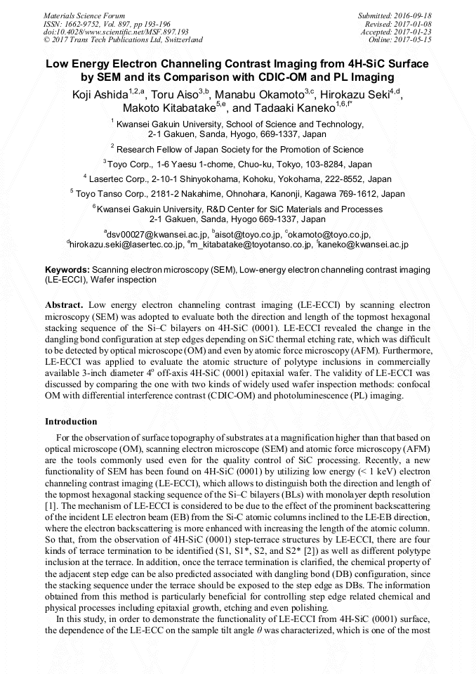
Low Energy Electron Channeling Contrast Imaging from 4H-SiC Surface by SEM and its Comparison with CDIC-OM and PL Imaging
Abstract:
Low energy electron channeling contrast imaging (LE-ECCI) by scanning electron microscopy (SEM) was adopted to evaluate both the direction and length of the topmost hexagonal stacking sequence of the Si–C bilayers on 4H-SiC (0001). LE-ECCI revealed the change in the dangling bond configuration at step edges depending on SiC thermal etching rate, which was difficult to be detected by optical microscope (OM) and even by atomic force microscopy (AFM). Furthermore, LE-ECCI was applied to evaluate the atomic structure of polytype inclusions in commercially available 3-inch diameter 4o off-axis 4H-SiC (0001) epitaxial wafer. The validity of LE-ECCI was discussed by comparing the one with two kinds of widely used wafer inspection methods: confocal OM with differential interference contrast (CDIC-OM) and photoluminescence (PL) imaging.
Info:
Periodical:
Pages:
193-196
DOI:
Citation:
Online since:
May 2017
Authors:
Price:
Сopyright:
© 2017 Trans Tech Publications Ltd. All Rights Reserved
Share:
Citation:


