p.411
p.415
p.419
p.423
p.427
p.431
p.435
p.439
p.443
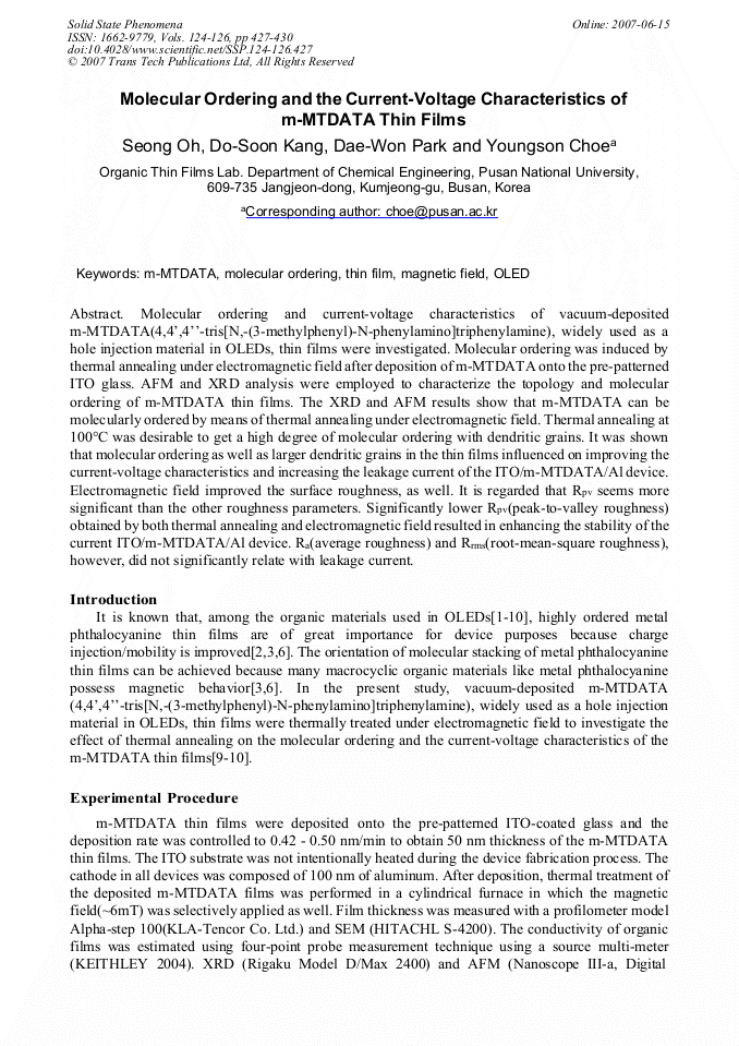
Molecular Ordering and the Current-Voltage Characteristics of m-MTDATA Thin Films
Abstract:
Molecular ordering and current-voltage characteristics of vacuum-deposited m-MTDATA(4,4’,4’’-tris[N,-(3-methylphenyl)-N-phenylamino]triphenylamine), widely used as a hole injection material in OLEDs, thin films were investigated. Molecular ordering was induced by thermal annealing under electromagnetic field after deposition of m-MTDATA onto the pre-patterned ITO glass. AFM and XRD analysis were employed to characterize the topology and molecular ordering of m-MTDATA thin films. The XRD and AFM results show that m-MTDATA can be molecularly ordered by means of thermal annealing under electromagnetic field. Thermal annealing at 100°C was desirable to get a high degree of molecular ordering with dendritic grains. It was shown that molecular ordering as well as larger dendritic grains in the thin films influenced on improving the current-voltage characteristics and increasing the leakage current of the ITO/m-MTDATA/Al device. Electromagnetic field improved the surface roughness, as well. It is regarded that Rpv seems more significant than the other roughness parameters. Significantly lower Rpv(peak-to-valley roughness) obtained by both thermal annealing and electromagnetic field resulted in enhancing the stability of the current ITO/m-MTDATA/Al device. Ra(average roughness) and Rrms(root-mean-square roughness), however, did not significantly relate with leakage current.
Info:
Periodical:
Pages:
427-430
Citation:
Online since:
June 2007
Authors:
Keywords:
Price:
Сopyright:
© 2007 Trans Tech Publications Ltd. All Rights Reserved
Share:
Citation:


