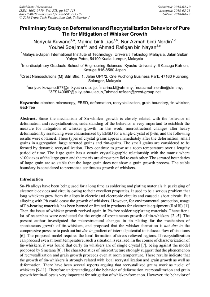
Preliminary Study on Deformation and Recrystallization Behavior of Pure Tin for Mitigation of Whisker Growth

Article Preview

Abstract:

Since the mechanism of Sn-whisker growth is closely related with the behavior of deformation and recrystallization, understanding of the behavior is very important to establish the measure for mitigation of whisker growth. In this work, microstructural changes after heavy deformation by scratching were characterized by EBSD for a single crystal of β-Sn, and the following results were obtained. Three types of crystal grains appear immediately after the deformation; small grains in aggregation, large serrated grains and rim-grains. The small grains are considered to be formed by dynamic recrystallization. They continue to grow at a room temperature over a lengthy period of time. The large grain has a certain crystallographic relationship with the matrix where <100> axes of the large grain and the matrix are almost parallel to each other. The serrated boundaries of large grain are so stable that the large grain does not show a grain growth process. The stable boundary is considered to promote a continuous growth of whiskers.

You might also be interested in these eBooks

Info:

Periodical:

Solid State Phenomena (Volume 273)

Pages:

107-111

Citation:

Online since:

April 2018

Export:

Price:

Permissions CCC:

Permissions PLS:

Сopyright:

© 2018 Trans Tech Publications Ltd. All Rights Reserved

Share:

Citation:

[1] European Parliament. Proposal for a Directive of the European Parliament and of the Council on Waste Electrical and Electronic Equipment and on the Restriction of the use of Certain Hazardous Substances in Electronic Equipment. COM 2000: 347.

Google Scholar

[2] C. Xu, Y. Zhang, C. Fan and J. A. Abys: IEEE Trans. Electronics Packaging Manufacturing, vol. 28 (2005), p.31.

Google Scholar

[3] S-B. Li, G-P. Bei, H-X Zhai, Z-I Zhang, Y. Zhou and C-W. Li: J. Mater. Res., Vol. 22 (2005), p.31.

Google Scholar

[4] H. Moriuchi, Y. Tadokoro, M. Sato, T. Furusawa and N. Suzuki: J. Electronic Mater. Vol. 36 (2007), p.220.

Google Scholar

[5] K. Suganuma: J. Surface Finishing Society of Japan, Vol 59(2008), p.210 (in Japanese).

Google Scholar

[6] N. Kuwano and Marina binti Lias: Proceedings of Malaysia-Japan Joint International Conference 2016, Kuala Lumpur, MJIIT, UTM, MJ2-MPE_2, 170305153.

DOI: 10.35940/ijrte.d9934.118419

Google Scholar

[7] N. Kuwano, S. Horikami and Marina Linas: Mater. Sci. Forum, Vol. 827 (2015), p.341.

Google Scholar

[8] J. Smetana: IEEE Trans. Electr. Pack. Manuf. Vol. 30 (2007), p.11.

Google Scholar

[9] P. T. Vianco and J. A. Rejent: J. Electronic Mater. Vol. 38 (2009), p.1815.

Google Scholar

[10] B. Honváth, B. Illés, T. Shinohara and G. Harsány: Materials Letters, Vol. 99 (2013), p.76.

Google Scholar

[11] J. Chang, S. K. Kang, J-H. Lee, K-S. Kim and H-M. Lee: J. Electronic Mater. Vol.44 (2015), p.3486.

Google Scholar

[12] Marina Lias and N. Kuwano: Proceedings of the MJIIT-JUC Joint International Symposium 2013, (2013), MP-034. MJIIT, UTM (Kuala Lumpur).

DOI: 10.35940/ijrte.d9934.118419

Google Scholar