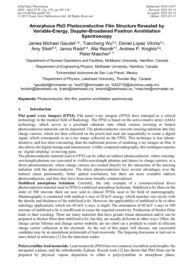
Amorphous PbO Photoconductive Film Structure Revealed by Variable-Energy, Doppler-Broadened Positron Annihilation Spectroscopy

Article Preview

Abstract:

Photoconductive amorphous selenium (a-Se) layers are utilized in flat panel X-ray imaging detectors as a direct conversion medium, converting X-ray photons directly into electric charge. Commercial a-Se direct conversion Active Matrix Flat Panel Imagers (AMFPIs) have demonstrated superior image quality in mammography, showcasing the potential of this X-ray imaging technology [1-2]. The use of a-Se is limited, however, by its low Z, resulting in low stopping of high energy X-rays [2]. This limitation is not shared by PbO thin films. Earlier PbO films consisted of small poly-crystalline platelets with low film density and suffered from the presence of both oxygen vacancies and impurity phases (PbO2). Recent advances [3-4] have yielded dense amorphous PbO (a-PbO) films with apparently uniform stoichiometry, as confirmed by X-ray photoelectron spectroscopy (XPS). More careful analysis [5] using X-ray absorption spectroscopy (XAS) indicated some tailing of the conduction band, which was attributed to suspected O-vacancies. An annealing study on a-PbO [3] indicated a transition to β-PbO around 500 C. X-ray diffraction (XRD) data of the β-PbO (annealed a-PbO) film matched that of a β-PbO reference, while XAS data did not. This was attributed to the different depths of the sample volumes probed by the two techniques. Doppler-broadened positron annihilation spectroscopy (DBPAS) was conducted on several a-PbO samples synthesized under different conditions using the McMaster Variable-Energy Positron Beam (MVEPB) and the results were modelled using VEPFIT [6]. All samples were found to have a three-layer structure, with the bulk S-parameters between 0.4725 and 0.4753. The two other layers were contained within the first 300nm of the film and varied in thickness, diffusion length and S-parameter value. This confirms the suitability of DBPAS, as a sensitive probe of vacancy-type defects and the layer structure of thin films, to guide the optimization of a-PbO synthesis for photoconductive detectors. Work is underway to produce a series of samples which vary systematically in their synthesis conditions to establish synthesis-structure relationships.

You might also be interested in these eBooks

Info:

Periodical:

Solid State Phenomena (Volume 374)

Pages:

103-118

Citation:

Online since:

July 2025

Export:

Price:

Permissions CCC:

Permissions PLS:

Сopyright:

© 2025 Trans Tech Publications Ltd. All Rights Reserved

Share:

Citation:

* - Corresponding Author

[1] Amorphous and Polycrystalline Photoconductors for Direct Conversion Flat Panel X-Ray Image Sensors. Kasap, Safa, et al. May 09, 2011, Sensors, Vol. 11, pp.5112-5157.

DOI: 10.3390/s110505112

Google Scholar

[2] Ion-assisted deposition of amorphous PbO layers. Semeniuk, O., et al. New York: Springer, March 22, 2017, Journal of Materials Science.

Google Scholar

[3] In Situ Characterization of Metastable Pb3O5 and Pb2O3 Phases During Thermal Decomposition of PbO2 to PbO. Kinnibrugh, Tiffany L., et al. s.l. : ACS Publications, July 25, 2024, Inorganic Chemistry, Vol. 63, pp.14313-14324.

DOI: 10.1021/acs.inorgchem.3c04482.s001

Google Scholar

[4] X-ray spectroscopic study of amorphous and polycrystalline PbO films, alpha-PbO, and beta-PbO for direct conversion imaging. Qamar, A., et al. s.l. : Springer Nature, October 13, 2017, Scientific Reports, Vol. 7, p.13159.

DOI: 10.1038/s41598-017-13703-7

Google Scholar

[5] A Probe of Valence and Conduction Band Electronic Structure of Lead Oxide Films for Photo-detectors. Qamar, Amir, et al. [ed.] Kira Welter. Weinheim : European Chemical Societies Publishing, 2019, ChemPhysChem.

Google Scholar

[6] Comparative Analysis of Multilayer Lead Oxide-Based X-ray Detector Prototypes. Pineau, Emma, et al. [ed.] Leonardo Abbene. Basel : MDPI, August 11, 2022, Sensors, Vol. 22, p.5998.

DOI: 10.3390/s22165998

Google Scholar

[7] A Na-22 positron source for use in UHV. Krause-Rehberg, R., et al. s.l. : Elsevier, 2004, Nuclear Instruments and Methods in Physics Research B, Vol. 221, p.165–167.

DOI: 10.1016/j.nimb.2004.03.049

Google Scholar

[8] Improved Slow-Positron Yield Using a Single Crystal Tungsten Moderator. Vehanen, A., et al. s.l. : Springer-Verlag, 1983, Applied Physics A, Vol. 32, pp.163-167.

DOI: 10.1007/bf00616613

Google Scholar

[9] Positron-Beam Techniques for Materials Characterization. Lawther, Derek W. and Simpson, Peter J. March 1996, Defect and Diffusion Forum, Vols. 138-139, pp.1-18.

DOI: 10.4028/www.scientific.net/ddf.138-139.1

Google Scholar

[10] Lefebvre, Loïc. [Online] https://pymodbustcp.readthedocs.io/en/latest/.

Google Scholar

[11] ANALYSIS OF POSITRON PROFILING DATA BY MEANS OF 'VEPFIT". van Veen, A., et al. 1, s.l. : AIP Publisher, 1991, AIP Conference Proceedings, Vol. 218, p.171–198.

DOI: 10.1063/1.40182

Google Scholar

[12] Identification of vacancy defect complexes in transparent semiconducting oxides ZnO, In2O3 and SnO2. Makkonen, Ilja, et al. s.l. : IOP Publishing Ltd, March 08, 2016, Journal of Physics: Condensed Matter, Vol. 28, p.224002.

DOI: 10.1088/0953-8984/28/22/224002

Google Scholar