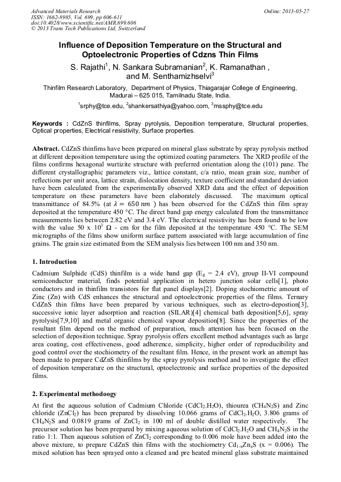
Influence of Deposition Temperature on the Structural and Optoelectronic Properties of CdZnS Thin Films

Article Preview

Abstract:

CdZnS thinfims have been prepared on mineral glass substrate by spray pyrolysis method at different deposition temperature using the optimized coating parameters. The XRD profile of the films confirms hexagonal wurtizite structure with preferred orientation along the (101) pane. The different crystallographic parameters viz., lattice constant, c/a ratio, mean grain size, number of reflections per unit area, lattice strain, dislocation density, texture coefficient and standard deviation have been calculated from the experimentally observed XRD data and the effect of deposition temperature on these parameters have been elaborately discussed. The maximum optical transmittance of 84.5% (at λ= 650 nm ) has been observed for the CdZnS thin film spray deposited at the temperature 450 °C. The direct band gap energy calculated from the transmittance measurements lies between 2.82 eV and 3.4 eV. The electrical resistivity has been found to be low with the value 50 x 103 Ω - cm for the film deposited at the temperature 450 °C. The SEM micrographs of the films show uniform surface pattern associated with large accumulation of fine grains. The grain size estimated from the SEM analysis lies between 100 nm and 350 nm.

You might also be interested in these eBooks

Info:

Periodical:

Pages:

606-611

Citation:

Online since:

May 2013

Export:

Price:

Permissions CCC:

Permissions PLS:

Сopyright:

© 2013 Trans Tech Publications Ltd. All Rights Reserved

Share:

Citation:

[1] Ichimura M., Goto F., Arai E., "Structural and Optical Characterization of CdS Films Grown by Photochemical Deposition", J. Appl. Phys. 85, (1999) 7411-7419.

DOI: 10.1063/1.369371

Google Scholar

[2] Bilgin V., Kose S., Atay F., Akyuz I., 2005. "The Effect of Substrate Temperature on the Structural and Some Physical Properties of Ultrasonically Sprayed CdS Films", Materials Chemistry and Physics, 94, (2005)103-108.

DOI: 10.1016/j.matchemphys.2005.04.028

Google Scholar

[3] A.A. Al bassan, Photoconductivity and defect levels in ZnxCd1-xSe with (x=0.5, 0.55) crystals, Solar Energy Mater. Sol. Cells 57, (1999) 329.

DOI: 10.1016/s0927-0248(98)00154-8

Google Scholar

[4] G. Laukaitish, S. Lindroos, S. Tamulevicius, M.Leskela, M. Rackitis, Successive ionic layer adsorption and reaction, Appl. Surf. Sci. 161, (2000) 396.

Google Scholar

[5] P. U. Asogwa, variation of optical properties with post deposition annealing in chemically deposited CdZnS thin films, Chalcogenide Letters, Vol. 7, No. 8, (2010) 501 - 508.

Google Scholar

[6] T. Prem kumar, K. Sankaranarayanan, Growth and characterization of CdZnS thin films by short duration micro wave assisted-chemical bath deposition technique, Chalcogenide Letters, Vol. 6, No. 10, (2009) 555 – 562.

Google Scholar

[7] L.S. Ravangave, U.V. Biradar, S.D. Misal, The effect of ionic composition and Optical properties of CdxZn1-xS thin films grown by spray pyrolysis, Int. Jour. Of Sci. and Research Publications, Vol. 2, Issue 6, (2012)1-5.

Google Scholar

[8] Patricia B. Smith, Low temperature, low pressure CdZnS films produced by metalorganic chemical vapour deposition, J. Vac. Sci. Technol. A 10, (1992) 897.

DOI: 10.1116/1.577691

Google Scholar

[9] Y. Raviprakash, V. Kasturi, V. Bangera and G. K. Shivakumar, Preparation and characterization of CdxZn1-xS thin films by spray pyrolysis technique for photovoltaic applications, solar energy, Vol. 83, (2009) 1645 – 1651.

DOI: 10.1016/j.solener.2009.06.004

Google Scholar

[10] Metin Bedir, Refik Kayali and Mustafa oztas, effect of the Zn concentration on the characteristic parameters of ZnxCd1-xS thin films developed by spraying pyrolysis method under the Nitrogen atmosphere, Turk J. Phys. Vol. 26, (2002) 121 – 126.

Google Scholar