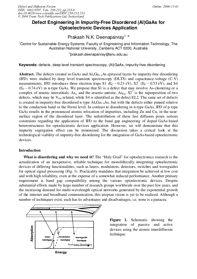
[1]
J.J. Coleman, R.M. Lambert, M.L. Osowski and A.M. Jones: IEEE J. Sel. Top. Quantum Electron. Vol 3 (1997), p.874, and references therein.
Google Scholar
[2]
R.M. Cohen: Mater. Sci. Eng. R Vol 20 (1997), p.167.
Google Scholar
[3]
A. Saher Helmy, J.S. Aitchison and J.H. Marsh: Appl. Phys. Lett. Vol 71 (1997), p.2998.
Google Scholar
[4]
W.P. Gillin: Semiconductor Quantum Wells Intermixing - Optoelectronic Properties of Semiconductors and Superlattices, Vol 8, Ed. E. Herbert Li (Gordon and Breach, The Netherlands 2000), pp.53-84.
Google Scholar
[5]
For a comprehensive review of disordering techniques see, Semiconductor Quantum Wells Intermixing - Optoelectronic Properties of Semiconductors and Superlattices, Vol 8, Ed. E. Herbert Li (Gordon and Breach, The Netherlands 2000).
Google Scholar
[6]
J.H. Marsh: Semicond. Sci. Technol. Vol 8 (1993), p.1136.
Google Scholar
[7]
A. Pépin, C. Vieu, M. Schneider, H. Launois and Y. Nissim: J. Vac. Sci. Technol. B Vol 15 (1997), p.142.
Google Scholar
[8]
L. Fu, J. Wong-Leung, P.N.K. Deenapanray, H.H. Tan, C. Jagadish, Bin Gong, R.N. Lamb, R.M. Cohen, W. Reichert, L. V. Dao and M. Gal: J. Appl. Phys. Vol 92 (2002), p.3579.
DOI: 10.1063/1.1503857
Google Scholar
[9]
H.G. Grimmeiss: Ann. Rev. Mater. Sci. Vol 7 (1977), p.341.
Google Scholar
[10]
J.W. Corbett, J.P. Karins and T.Y. Tan, Nucl. Instrum. Methods Vol 182-183 (1981), p.457.
Google Scholar
[11]
Y. Zohta and M.O. Watanabe: J. Appl. Phys. Vol 53 (1982), p.1890.
Google Scholar
[12]
H. Lefevre and M. Schultz: Appl. Phys. Vol 12 (1977), p.45.
Google Scholar
[13]
P.N.K. Deenapanray, V.A. Coleman and C. Jagadish: Electrochem. Solid-State Lett. Vol 6 (2003), p. G37.
Google Scholar
[14]
A. Mitonneau, G.M. Martin and A. Mircea: Electron. Lett. Vol 13 (1977), p.666.
Google Scholar
[15]
D. Stievenard, X. Boddaert and J.C. Bourgoin: Phys. Rev. B Vol 34 (1986), p.4048.
Google Scholar
[16]
J. Lagowski, D.G. Lin, T. -P. Cehn, M. Skowronski and H.C. Gatos: Appl. Phys. Lett. Vol 47 (1985), p.929.
Google Scholar
[17]
G. Hofmann, J. Madok, N.M. Naegel, G. Roos, N.M. Johnson and E.E. Haller: Appl. Phys. Lett. Vol 61 (1992), p.2914.
Google Scholar
[18]
Z.G. Wang, H.P. Gislason and B. Monemar: J. Appl. Phys. Vol 58 (1985), p.230.
Google Scholar
[19]
M. Luysberg, W. Jäger, K. Urban, M. Schänzer, N.A. Stolwijk and H. Mehrer: Mater. Sci. Engn. B Vol 13 (1992), p.137.
Google Scholar
[20]
P.W. Hutchinson and R.K. Ball: J. Mater. Sci. Vol 17 (1982), p.406.
Google Scholar
[21]
Y.C. Lu, T.S. Kalkur and C.A. Paz de Araujo: J. Electron. Mater. Vol 19 (1990), p.29.
Google Scholar
[22]
R. Leon, P. Werner, K.M. Yu, M. Kaminska and E.R. Weber: Appl. Phys. A Vol 61 (1995), p.7.
Google Scholar
[23]
S. Yu, T.Y. Tan and U. Gösele: J. Appl. Phys. Vol 69 (1991), p.3547.
Google Scholar
[24]
G. Bösker, N.A. Stolwijk, H. -G. Hettwer, A. Rucki, W. Jäger and U. Södervall: Phys. Rev. B Vol 52 (1995), p.11927.
DOI: 10.1103/physrevb.52.11927
Google Scholar
[25]
F.C. Frank and D. Turnbull: Phys. Rev. Vol 104 (1981), p.617.
Google Scholar
[26]
G. Rajeswaran, K.B. Kahen and D.J. Lawrence: J. Appl. Phys. Vol 69 (1991), p.1359.
Google Scholar
[27]
R. Krause-Rehberg, K. Petters and J. Gebauer: Physica B Vol 273-274 (1999), p.714.
Google Scholar
[28]
M. Buda, J. Hay, H.H. Tan, L. Fu, C. Jagadish, P. Reece and M. Gal: J. Electrochem. Soc. Vol 150 (2003), p. G481.
DOI: 10.1149/1.1588304
Google Scholar
[29]
D.G. Deppe and N. Holonyak, Jr.: J. Appl. Phys. Vol 64 (1988), p. R93.
Google Scholar
[30]
P.N.K. Deenapanray, H.H. Tan, C. Jagadish and F. D. Auret: J. Appl. Phys. Vol 88 (2000), p.5255.
Google Scholar
[31]
H.J. von Bardeleben, D. Stiévenard, D. Deresmes, A. Huber and J.C. Bourgoin: Phys. Rev. B Vol 34 (1986), p.7192.
DOI: 10.1103/physrevb.34.7192
Google Scholar
[32]
A. Ito, A. Kitagawa, Y. Tokuda, A. Usami, H. Kano, H. Noge and T. Wada: Semicond. Sci. Technol. Vol 4 (1989), p.416.
Google Scholar
[33]
P.N.K. Deenapanray, Bin Gong, R.N. Lamb, A. Martin, L. Fu, H.H. Tan and C. Jagadish: Appl. Phys. Lett. Vol 80 (2002), p.4351.
Google Scholar
[34]
S. Makram-Ebeid, D. Gautard, P. Devillard and G.M. Martin: Appl. Phys. Lett. Vol 40 (1982), p. (1982).
DOI: 10.1063/1.93028
Google Scholar
[35]
P.N.K. Deenapanray, W.E. Meyer, F. D. Auret, M. Krispin and C. Jagadish: Physica B Vol 340-342 (2003), p.315.
DOI: 10.1016/j.physb.2003.09.084
Google Scholar
[36]
P.N.K. Deenapanray, M. Lay, D. Åberg, H.H. Tan, B.G. Svensson, F.D. Auret and C. Jagadish: Physica B Vol 308-310 (2001), p.776.
DOI: 10.1016/s0921-4526(01)00836-5
Google Scholar
[37]
S. Doshi, P.N.K. Deenapanray, H.H. Tan and C. Jagadish: J. Vac. Sci. Technol. B Vol 21 (2003), p.198.
Google Scholar
[38]
J.I. Landman, C.G. Morgan, J.T. Schick, P. Papoulias and A. Kumar: Phys. Rev. B Vol 55 (1997), p.15581.
Google Scholar
[39]
M. Stellmacher, R. Bisaro, P. Galtier, J. Nagle, K. Khirouni and J.C. Bourgoin: Semicond. Sci. Technol. Vol 16 (2001), p.440.
DOI: 10.1088/0268-1242/16/6/304
Google Scholar
[40]
G. Zollo and R.M. Nieminen: J. Phys.: Condens. Matter Vol 15 (2003), p.843.
Google Scholar
[41]
M.H. Zhang, L.W. Guo, H.W. Li, W. Li, Q. Huang, C.L. Bao, J.M. Zhou, B.L. Liu, Z.Y. Xu, Y.H. Zhang and L.W. Lu: Phys. Rev. B Vol 63 (2001), p.115324.
Google Scholar
[42]
T.E.M. Staab, R.M. Nieminen, M. Luysberg, J. Gebauer and Th. Frauenheim: Physica B Vol 340-342 (2003), p.293.
DOI: 10.1016/j.physb.2003.09.088
Google Scholar
[43]
P.N.K. Deenapanray and F.D. Auret: unpublished.
Google Scholar
[44]
M. Kuzuhara, T. Nozaki and T. Kamejima: J. Appl. Phys. Vol 66 (1989), p.5833.
Google Scholar
[45]
P.N.K. Deenapanray, H.H. Tan, C. Jagadish and F. D. Auret: Appl. Phys. Lett. Vol 77 (2000), p.626.
Google Scholar
[46]
J.A. Van Vechten: J. Phys.: Condens. Matter Vol 1 (1989), p.5171.
Google Scholar
[47]
T. Laine, J. Mäkinen, K. Saarinen, P. Hautojärvi, C. Corbel and P. Gibart: Mater. Sci. Forum Vol 196-201 (1995), p.1073.
DOI: 10.4028/www.scientific.net/msf.196-201.1073
Google Scholar