p.269
p.274
p.279
p.284
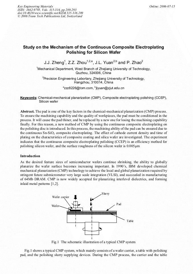
p.289
p.294
p.299
p.304
p.309
Study on the Mechanism of the Continuous Composite Electroplating Polishing for Silicon Wafer

Abstract:
The pad is one of the key factors in the chemical-mechanical planarization (CMP) process. To ensure the machining capability and the quality of workpieces, the pad must be conditioned in the process. It will cause the pad thiner, and be replaced by a new one for losing the machining capability finally. For this reason, a new method of CMP by using the continuous composite electroplating on the polishing disc is introduced. In this process, the machining ability of the pad can be ensured due to the continuous Sn-SiO2 composite electroplating. The effect of cathode current density and time of plating on the characteristics of composite coating and silica wafer are investigated. The experiment indicates that the continuous composite electroplating polishing (CCEP) is an efficiency method for polishing silicon wafer, and the surface roughness of the silicon wafer is 0.005μm
Info:
Periodical:
Pages:
289-293
Citation:
Online since:
July 2006
Authors:
Price:
Сopyright:
© 2006 Trans Tech Publications Ltd. All Rights Reserved
Share:
Citation: