Fabrication and Characteristics of the Nano-Polysilicon Thin Film Transistors

Article Preview

Abstract:

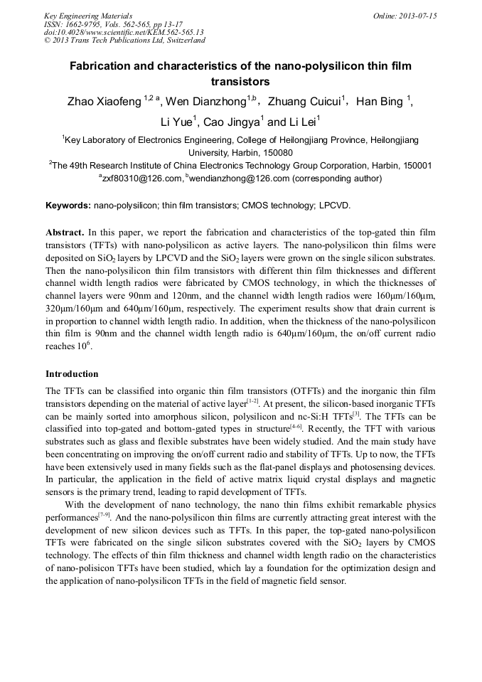
In this paper, we report the fabrication and characteristics of the top-gated thin film transistors (TFTs) with nanopolysilicon as active layers. The nanopolysilicon thin films were deposited on SiO2 layers by LPCVD and the SiO2 layers were grown on the single silicon substrates. Then the nanopolysilicon thin film transistors with different thin film thicknesses and different channel width length radios were fabricated by CMOS technology, in which the thicknesses of channel layers were 90nm and 120nm, and the channel width length radios were 160μm/160μm, 320μm/160μm and 640μm/160μm, respectively. The experiment results show that drain current is in proportion to channel width length radio. In addition, when the thickness of the nanopolysilicon thin film is 90nm and the channel width length radio is 640μm/160μm, the on/off current radio reaches 106.

You might also be interested in these eBooks

Info:

Periodical:

Key Engineering Materials (Volumes 562-565)

Pages:

13-17

Citation:

Online since:

July 2013

Export:

Price:

Permissions CCC:

Permissions PLS:

Сopyright:

© 2013 Trans Tech Publications Ltd. All Rights Reserved

Share:

Citation:

[1] A. Cerdeira, M. Estrada, B. Iñiguez, et al, Modeling and parameterextraction procedure for nanocrystalline TFTs, J. Solid-State Electronics. 48(2004) 102- 609.

DOI: 10.1016/s0038-1101(03)00267-3

Google Scholar

[2] S.F. Chen, Y.K. Fang, T.H. Lee, et al, Enhancing the crystallization fraction performance of nano-crystalline silicon thin films with argon and hydrogen annealing, J. Thin Solid Films. 515(2007) 3842-8846.

DOI: 10.1016/j.tsf.2006.10.075

Google Scholar

[3] Tamila Aliyeva Anutgan, Mustafa Anutgan, Ismail Atilgan, et al, Large area uniformity of plasma grown hydrogenated nanocrystalline silicon and its application in TFTs, J. Journal of Nancrystalline Solids. 356(2010) 1102-1108.

DOI: 10.1016/j.jnoncrysol.2010.04.012

Google Scholar

[4] Li.Flora, Sazonov.Andrei,Nathan, Arokia.Stability of Nanocrystalline Silicon Bottom-gate Thin Film Transistors with Silicon Nitride Gate Dielectric, J. Journal of Applied Physics. 102 (2007) 064512-064512-7.

DOI: 10.1063/1.2784008

Google Scholar

[5] Youn-Jin Lee, Kyoung-Min Lee, Wan-Shick Hong, Characteristics of bottom-gate low temperature nanocrystalline silicon thin film transistor fabricated by hydrogen annealing of gate dielectric layer, J. Thin Solid Films. 518(2010) 6311-6314.

DOI: 10.1016/j.tsf.2010.03.057

Google Scholar

[6] Masaki Hara, High mobility bottom gate nanocrystalline-Si thin-film transistors, J. Thin Solid Films. 519(2011) 3922-3924.

DOI: 10.1016/j.tsf.2011.01.283

Google Scholar

[7] A. LeDonne, S. Binetti, B. Pichaud, et al, Structural characterization of nc-Si films grown by low-energy PECVD on different substrates, J. Applied Surface Science. 254(2008) 2804-2808.

DOI: 10.1016/j.apsusc.2007.10.025

Google Scholar

[8] M.Yoshikawa, M.Muarkami, K.Matsuda, et al, Characterization of Si nano-polycrystalline films at the nanometer level using resonant Raman scattering, J. Journal of Applied Physics. 98(2005) 063531-1-063531-6.

DOI: 10.1063/1.2060954

Google Scholar

[9] A.A.D.T. Adikaari, S.R.P. Silva, Thickness dependence of properties of excimer laser crystallized nano-polycrystalline silicon, J. Journal of Applied Physics. 97(2005) 114305-1- 114305-6.

DOI: 10.1063/1.1898444

Google Scholar