p.921
p.925
p.929
p.934
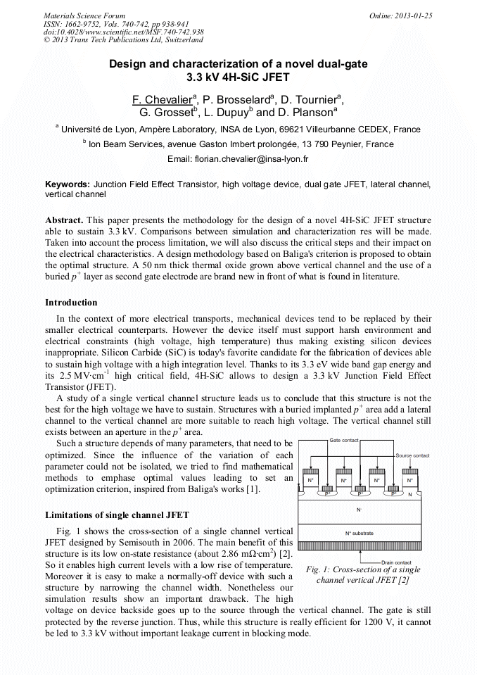
p.938
p.942
p.946
p.950
p.954
Design and Characterization of a Novel Dual-Gate 3.3 Kv 4H-Sic JFET

Abstract:
This paper presents the methodology for the design of a novel 4H-SiC JFET structure able to sustain 3.3 kV. Comparisons between simulation and characterization res will be made. Taken into account the process limitation, we will also discuss the critical steps and their impact on the electrical characteristics. A design methodology based on Baliga's criterion is proposed to obtain the optimal structure. A 50 nm thick thermal oxide grown above vertical channel and the use of a buried p+ layer as second gate electrode are brand new in front of what is found in literature.
Info:
Periodical:
Pages:
938-941
Citation:
Online since:
January 2013
Authors:
Price:
Сopyright:
© 2013 Trans Tech Publications Ltd. All Rights Reserved
Share:
Citation: